Testing of the Fox JITO-2 Oscillator as the N2PK VNA Master Oscillator

Oscillator Description:

  • Type: Fox JITO-2-P
  • P/N: PC5BF-148.344
  • Frequency: 148.344 MHz
  • Output levels: HCMOS
  • Power: +5.0 VDC
  • Frequency stability: +/-50 ppm
  • Operating Temp: -20 to +70 C
  • URL: http://www.foxonline.com/jito_p.htm
Test Summary:
  • JITO-2 in the VNA Master Oscillator Test Board.
    • Result: Functional - it properly switches the 74AC74
  • JITO-2 in my prototype VNA. See its pix in Part 2, pg 19.
    • Result: Functional - DDSs are programmed to the correct frequencies & phases
  • Phase Noise of JITO-2 in my prototype VNA.
    • Result: Not suitable for high performance VNA usage - see table, plots and discussion below.

Phase Noise Test Methods:

  • A high purity 10 MHz VCXO was phase locked to the VNA RF DDS running at 10 MHz in a phase noise tester for all but the HBMO test.
  • The phase noise tester is similar in concept to "Demphano", as documented by Jacob Makhinson in Communications Quarterly, Spring 1999.
  • W4ZCB used a filter test method for the HBMO test with the DDS running at 10.2 MHz.

The table below summarizes the measured phase noise data for the following master oscillators and VNAs:

  • JITO-2 oscillator in my prototype VNA (JITO-2), tested 07/21/04.
  • Valpey-Fisher master oscillator (VFMO) in my PCB VNA per Part 2 of the VNA docs, tested 03/27/03.
  • Home brew master oscillator (HBMO) in W4ZCB's PCB VNA per Part 2 with the ICM low phase noise crystal, tested 03/24/03.
  • Prototype discrete master oscillator (PDMO) in my prototype VNA, tested 07/28/04. This oscillator is a bipolar Butler with no special phase noise requirements placed on its 130 MHz crystal.

The frequency column in the table is the offset from the carrier. In all cases, spurs were assumed to be due to the DDS or power line harmonics and were excluded where possible from these data. For the JITO-2, no spurs were noted due to its high phase noise.

The noise bandwidth was 7 Hz or less for all tests except W4ZCB's HBMO test, which was done at 50 Hz bandwidth.


Phase Noise, dBc/Hz
Freq, Hz JITO-2 VFMO HBMO PDMO
10 -85 N/A N/A -83
20 -83 -102 N/A -87
40 -81 -112 N/A -96
70 -80 -118 N/A -102
100 -79 -122 -120 -110
200 -78 -129 -120 -117
400 -76 -134 -130 -123
700 -74 -136 -134 -130
1000 -72 -136 -136 -134
2000 -71 -142 -137 -140
4000 -69 -144 -141 -145
7000 -69 -148 N/A -148
10000 -69 -151 -142 -150

Discussion:
  • More negative numbers are desirable for phase noise (see the ARRL Hamdbook).
  • The JITO-2 phase noise is about 60-80 dB worse than the Valpey-Fisher oscillator for offsets greater than 400 Hz where phase noise is likely to degrade dynamic range.
  • This substantially poorer phase noise is worse than what might be expected when comparing the 20 ps jitter specification for the JITO-2 oscillator vs. the 1 ps spec for the Valpey Fisher oscillator.
  • The somewhat better phase noise of the PDMO over the JITO-2 eliminates concerns that the dead-bug construction used in the prototype VNA causes significant phase noise degradation.

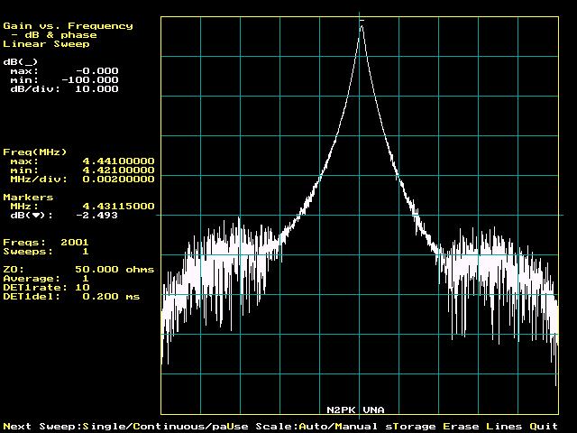
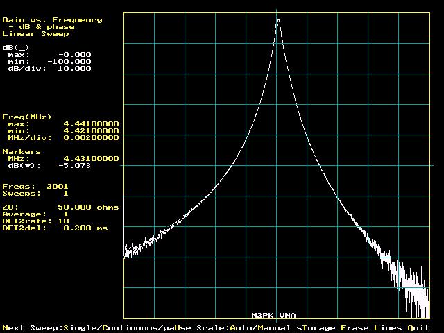
VNA Transmission Tests

  • A narrowband 4.431 MHz filter was swept for insertion loss using a VNA equipped with a Fox JITO-2 master oscillator and another VNA equipped with the Valpey Fisher master oscillator.
  • All sweeps were done over the same +/-10 kHz window approximately centered on the filter passband.
  • Each of these VNAs has a detector equipped with a new fast LTC2440 ADC, currently in beta test.
  • The LTC2440 ADC is capable of ten conversion rates. New software, also in beta test.allows the user to select the conversion rate.
  • The oscillators are compared for noise floor using the fastest and slowest ADC conversion rates.
  • All plots have the same frequency window and 0 to -100 dB vertical scale.
  • Data averaging was not used.
Test Results:
  • Fox JITO-2 master oscillator, prototype VNA, fastest ADC rate: JITO-2 MO @ Rate=10

  • Valpey Fisher master oscillator, PCB VNA, fastest ADC rate: V-F MO @ Rate=10

  • Fox JITO-2 master oscillator, prototype VNA, slowest ADC rate: JITO-2 MO @ Rate=1

  • Valpey Fisher master oscillator, PCB VNA, slowest ADC rate: V-F MO @ Rate=1
Discussion:
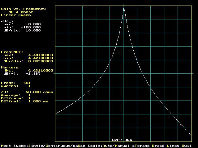
  • VNA dynamic range is degraded by about 30-35 dB at the fastest ADC conversion rate with the JITO-2 and an estimated 15-20 dB at the slowest ADC rate, both rates without averaging.
  • This loss in dynamic range will affect transmission measurements more than reflection (impedance) measurements which don't typically utilize the full dynamic range.
  • While not shown here, a test of the 4.431 MHz filter while averaging 10 ADC readings resulted in a 7 to 10 dB improvement in dynamic range at the fastest conversion rate. However, averaging dramatically increases the test time.
  • Exceptional reflection test cases might involve an active narrowband DUT which requires an attenuated input level to maintain linearity. In such a case, the poorer JITO-2 phase noise may degrade measurement accuracy at the higher ADC conversion rates. However, such a DUT would seem unlikely.
  • The degraded phase noise due to the JITO-2 master oscillator would likely preclude certain ancillary uses of the VNA such as IP3 and MDS testing.
Summary
The extent of VNA dynamic range degradation with very poor master oscillator phase noise was not anticipated when I wrote in Part 2:

"The master oscillator clocks both DDSs at the same times, every 6.74 ns approximately, in essentially lock-step fashion with the same jitter applied to both DDS outputs. Conventional VNA testing depends on relative phase, and relative phase between the two DDSs is preserved, given the various operative time constants generally encountered. The only exception that I can imagine would be a test of an extremely narrowband filter. Even that seems unlikely given the 5 Hz detector bandwidth."

The most severe degradation occurs where the ADC digitally controlled bandwidth is opened up to accomodate the higher ADC conversion rates.

What was essentially overlooked here was the fact that the master oscillator phase noise, as scaled to the DDS outputs, acts in combination with the offset passband of a narrowband DUT to magnify the phase noise of the RF DDS passed to the detector relative to the desired response - i.e. when the DDS frequency is not in the DUT passband. This noise response is also increased due to the wider digital (and analog) bandwidths when the ADC is running at its faster conversion rates (about 6 kHz noise bandwidth @ the fastest rate).

Back


Please feel free to contact me with any comments or questions at:

Image

73,
Paul Kiciak, N2PK

URL: http://n2pk.com/VNA/JitoPN.html
Last updated: 19 Oct. 2006
Copyright © 2003 - 2006