 Thanks
Denis for this info.
Thanks
Denis for this info.PIC-A-TUNE
This is NOT an official site.
June 25th 2010- added web page site for Paul Berkeley's PCB's.
Pauls PCB's,
some pictures. Paul Berkeley may have PCB's
available.
July 5, 2017 (notes added at end by builders, please read them also.)
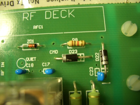
19th Sept. D23 is reversed on the PCB overlay!
9 & 14th Sept capacitor making ADDED
Sept 3rd, NEW Bill of material
May be slow to load as many pictures.
The designer of the PIC-A-TUNE auto antenna tuner for Amateur Radio is Peter, G3XJP, who published a series of articles describing his project in Radcom from Sept, 2000. to Jan 2001.
I understand that copies of Radcom may be obtained on a CD from the RSGB. (www.rsgb.org) Constructors are referred to the original article for details of the project, build information, set-up and use.
Original articles for PICaTUNE and Software may be obtained from the PICAPROJECT Yahoo group.
If you are NOT a member of that group you will need to join, as the schematics and build procedure are there also.
The purpose of this page is to provide additional information for the PCB's professionally made for the project made by VK3PE in July, 2008. Peter has allowed me to make these PCB's somewhat reluctantly, as he prefers builders to make their own PCB's for which artwork and details are available in the articles in Radcom.
The VK3PE PCB's follow the original designs as closely as possible with only minor variations to allow for some more current components. No SMD parts are used though.
Many thanks also to Chris S. for assisting me with these PCB's and drawings.
Bill of Material (BOM) (020908) PDF Format
NOTE: R26 on schematic is shown as R6 on the Logic board
This should reflect the original but with some possible sourcing information and component variations.
The general section of the BOM may not be 100% complete. There may be odd items you will need, so refer to the original article also.
The group buy of PCB's arrived late August, 2008 and have all been posted out. There may be a spare set available.
190908 NOTE: D23 on main PCB overlay is reversed. Photo shows correct fitting.
Thanks
Denis for this info.
What to do first !
When you start assembly, you need to remove all of the PCB sections from the panel, using, typically, a small a pair of side cutters to snip out the corners.
Then, with a small file, clean up the edges where they have been cut. Also, on the main PCB, file the two corners square, inside the notch where the SWR section will fit. There are four PCB's that make up the SWR housing and they fit into that "notch".
Check the hole sizes. Also, check for shorts. Details down the page.
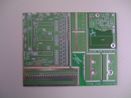 This
is the "logic" panel.
This
is the "logic" panel.
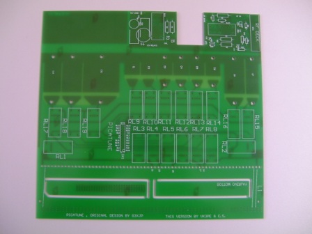 And the main board.
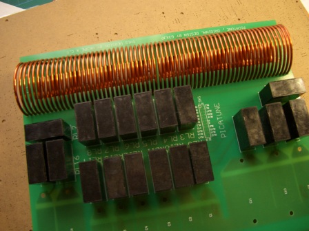
NOTE:- The main board has three rows of holes for fitting of L1. After you have wound L1 according to the information in the PICaTUNE articles, you need to decide which row of holes has to be opened out to fit L1. The suggested size is 2.5mm in the original article and L1 is made from 2mm wire. If you can find a drill of say, 2.2mm, start with that size and see if L1 can be fitted OK. I did not have all three holes drilled by the vendor as they would overlap each other.
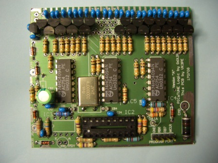
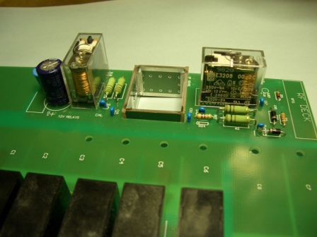
300808 I loaded up some parts I had:- Some parts are optional, marked as the A,B,C,D,E outputs. Refer to the original schematics and text.
Its a little tight to fit the 15uH choke on left side near the Electro. cap. Perhaps due to the size of the chokes or capacitor I used. In my case, I fitted it under the PCB which I think should be OK.
Not sure about the wisdom of using sockets in this project. I only used a socket for the PIC. Machined pin type would be much better.
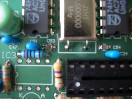
 The
top right hand two resistors should be 4k7 !
The
top right hand two resistors should be 4k7 !
You can fit 0805 SMD parts for the 100nF and 22pF capacitors if you want. Since I had the mono 100nF caps, I used them. Note that 0.1" pitch mono caps are used here. Usually you can buy either 0.1 or 0.2" pitch parts. Try to get the 0.1" parts if possible. Most Mono caps have 0.2" pitch but leads are easily reformed to 0.1". The main board (relay board) has dual pitch.
I used 0805 SMD for the C53 and C54 15pF parts. Sorry for the out of focus picture !
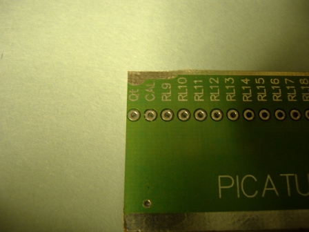
These pads (below) on the side of the Logic board are fairly close to the edge and may foul the side panels when you fit them (made from DS pcb material) Might be best to trim very slightly, the edge of the pad with a sharp knife on both sides of the pcb.
Picture added 6th Aug, 2008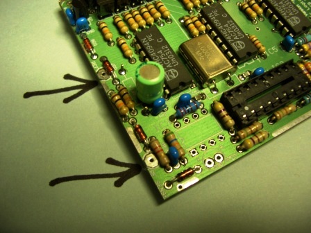
CAUTION!! Read Picatune manual for assembly order as not all parts are fitted when testing !!
17th Sept 2008, NOTE from Lawrence
16.09.2008 Glenn
I have checked them and there are a few points to check. R26 on the logic board is marked as R6. RL4 pad on logic board side connecter pcb strip is earthed on both sides when it should be open like the others, otherwise RL4 will stay on.
I had a couple of other bridges, one of them on the logic board transistors pads, so it is better to examine carefully or beep the pcb before populating to see whether everything is as it should be.
Otherwise all ok. Tnx & regards, Lawrence
I have built the main board a little out of order, in order to see if there are any problems with the PCB.
YES, the pcb vendor has not drilled some of the component holes the right size. Check before you start to mount any components but it appears to be limited to some of the resistors, the 20 pin connector and the two Electro. Caps. Use a 0.8mm drill.
The side plates for the SWR section are slightly too long. Most likely due to the errors in the routing. Fit the end PCB's first (when the time is appropriate) by LIGHTLY tacking them in, then fit the sides. Use a file to trim to length if needed. DON'T take too much off when you file. Just do a little at a time until you get a nice fit.
Make sure all the sides of the SWR section are at the same height and nice and square. Tack them only until completely satisfied with the fit.
See the note at the end of page, by Paul, re clearances
 Caution
see note above re D23 fitting !
Caution
see note above re D23 fitting !
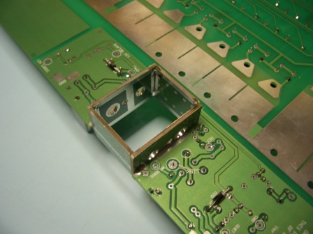
Another problem:- Check your PCB end plate. It is the PCB that will be fitted to the end of the LOGIC board.
On my PCB, there are etching problems. I found two pads connected to ground that should NOT be!! Pictured is one of them. The other is RL4 pad. Check yours with the beeper BEFORE you fit it. If you have shorts, they will need to be cleared with a sharp pointed knife, a Dremel tool or similar item.
You can see the little shorts in this picture: 2nd Pad from left side. (centre of picture) Another pad had problems also. Yours may be OK but CHECK all pads with Beeper . You may have problems on either side. Only one pad should connect to the copper (marked "GND")
I did not have problems on the other boards but it's a good idea to check all boards with the beeper and visually.
This PCB will eventually be soldered to the long pads on the end of the Logic board and be part of a box to shield the Logic board. The other sides you will need to make yourself from PCB material. I will show that later.
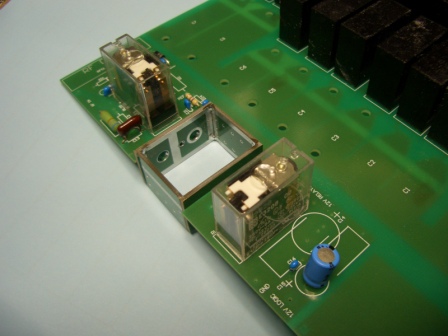
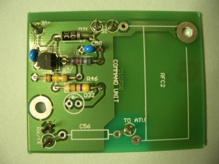
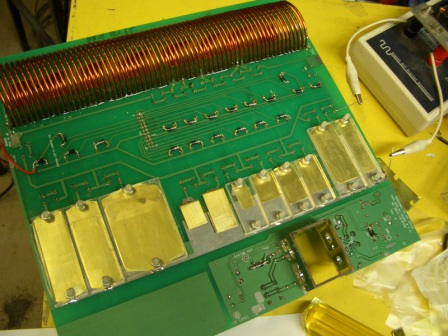
This is the Command board. This not an official PCB of Picatune but my own version of the Command schematic included in the the original documents. It is un-proven therefore. It will eventually be mounted in a shielded box. See the original article on PICaTUNE for details.
Still some parts to be fitted...............
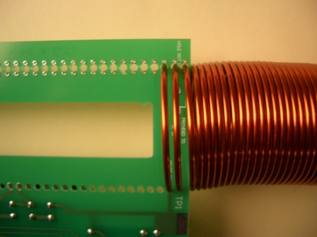
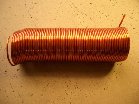
COIL WINDING
I am lucky in that I have a small lathe. I made a former from 40mm OD electrical conduit (ie plastic) and put the lathe on the slowest speed, then wound the coil while holding the wire with leather gloves, to keep it taught. It worked out very well, with a nice even coil and took less than 20 seconds to wind!
See note at end by Paul, re winding the coil, also
Be VERY CAREFUL if using a lathe. Have somebody ready to stop the lathe in case of problems.
But, it took me more than 30 minutes to insert it. It gets harder the further into the PCB. I used A 2.2mm drill to drill out the centre row of holes. Maybe 2.5mm would be a better idea, like the original by Peter.
You MUST check your OWN coil against the PCB, to see which holes YOU need to drill out.
You should also wind the coil into the PCB from the side that has extra holes which are marked "to provide ease of fitting L1". This also assumes you wind the coil in the correct rotational sense. eg my coil was wound on the former, from left to right. Its a little hard to explain but If you check the picture to the bottom, left, you will get the idea. It was wound into the PCB in a clockwise sense.
9th Sept, 2008: CAPACITOR MAKING
I started to make the capacitors and found it a bit tedious, to say the least, so some methods were developed to ease it a bit.
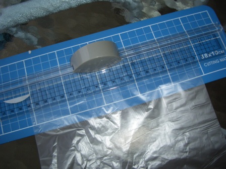
Cutting the freezer bags:-
I used a paper cutter to make the initial strips. This is a ruler that has a sliding cutting blade on the edge.
Cutting the Clamps:-
Before fitting any parts to the PCB or with a spare PCB, lay the plastic over the capacitor area, clamp to the PCB, and drill all the holes from the non copper side to avoid damage. Mark all the outlines of the clamps with a marking pen, then you can cut out all of the clamps with a jig saw etc.
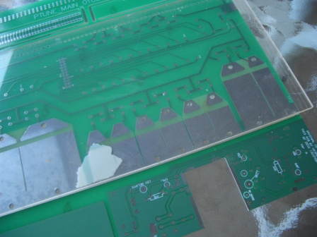
Also a drilling template (solder side) in case you already fitted parts to the PCB.
Make sure it's printed to scale. There is a 3 inch dimension on the drawing.
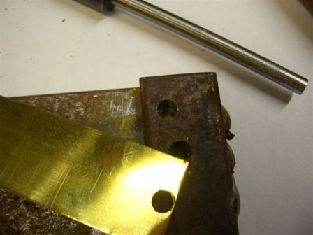
Drilling the Brass shim
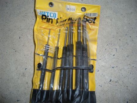
Drilling the brass is difficult. Peter's method may well work but I thought it may tear the hole edges and make it difficult to de burr the edges of the holes. I thought punching the holes would be better and as it happened, I have a cheap set of pin punches. Indeed, one was 4mm OD.
I made up a simple jig by welding two pieces of scrap steel together, with a gap between them. The same could be done by fastening together with small bolts and using a washer to space them apart. Then the 4mm hole is drilled. BUT you should use a 3mm hole first, then 4mm. The 4mm should be very sharp, to get a nice clean hole. Debur the holes with a flat file, then pass the drill through again. (Don't countersink them) The jig should be nice and clean, not rusty, like my example! I later cleaned it up.
The brass shim is cut to size first, then inserted into the jig, and the pin punch is driven through the hole with a quick tap of a hammer, to obtain a nice, near burr free hole.
Lacking a pin punch, the blunt end of an old 4mm drill bit could be used if the end is ground flat..
14th Sept, 2008: Making the Caps !
I have started to make the Capacitors.
This is proving a little frustrating. While the basic information is in the RTFM, so far, I must be having an interpretation problem, as I have a fair way to go to get them all somewhere near the correct values, mostly C3 to C6. The actual adjustment procedure seems to be missing or I need to re-read it again for the 10th time !
This is very messy and fiddly work. You need some dedication and lots of time to complete the job.
(don't copy mine, as its not finished yet)
9th Sept, 2008: Programming the PIC
Be aware that if you elect to use the PIC16F627 in your Picatune, you need to load the EEPROM on the Logic board, using a specially programmed PIC Loader, first. This code (by Peter, G3XJP) is only written for a PIC16F84 and is the "EP50_04.hex" code. This code cannot be used for the 16F627. Chris is modifying this code for the 16F627.
Check Yahoo "homebrew-radios" group.
Once the EP50_04 code is run to initialize the EEPROM (24C32) then the final code is then loaded into the PIC. Code is provided by Peter on PICAPROJECT pages for either the 16F84 or the 16F627.
NOTES FROM OTHER PICATUNE BUILDERS:-
Hi Glenn
A few of observations for you that I have encountered in my build -
(1) I wound L1 on my Myford lathe using slowest back gear (27RPM). I used a solid aluminium bar mandril turned to 42mm diameter with the wire anchored in a 2.5mm dimeter cross drilled hole. Using gloves to apply tension I achieved a finished coil diameter to suit the board's 46mm hole spacing option. With the outer holes drilled 2.3mm clear, the coil wound straight in with no binding at all. One important point is to make sure that extra turns are wound on to the mandril ( I wound 70 turns) as several turns are lost when the coil springs to its natural larger diameter.
(2) I have found on my RF deck board that the pad adjacent the SWR head notch leading to the R4/R5 junction is extremely close to the ground track of the SWR box (a condition which I exasperated by cutting the notch slightly wider to accomodate the box width as supplied). Bearing in mind that this pad will be subject to full TX power, I have elected to cut this track back to leave adequate spacing between it and ground. (3) On the logic board I have used turned pin sockets for IC 4, 5 and 6 because Peter's set up instructions require you to leave these IC's out until the final stages of set up.
Hope some of this helps
Kind regards & 73 de Paul M1PVC (210908)
If you have any queries, E-mail me.
8th Aug, 2008: PCB assembly information:
Logic board panel component overlay by ref # (R6 should be R26)
Logic board overlay by component value
Main board by ref # (refer to schematic for values) I will try to add a compont value version later.
This drawing shows some possible ways to connect the Logic Board:-
Logic Board interconnect details (added 12th Aug, 2008 by Chris)
There is an additional PCB in the area of L1, which is removed with side cutters. It has 2 rows of holes and tracks joining them. It can be used as per the drawing above if you wish.
More information on interconnect coming later............
Idea for "Improvement" (for the CW challenged !)
I had this idea that Picatune software could very easily (for PIC people) be modified to also have a serial output of status, fed to one of those little low power low speed data transmitter modules for a remote (ie at the Shack) display on a LCD module. The receiver would be the mating Rx unit with another PIC to get the data and display it on the LCD
. These little Tx and Rx modules are available in Australia in a low power unlicensed band for around $10 each. I don't know the viability in other countries though. They are about the size of a postage stamp.
Picatune >>>>>>>
Tx 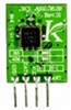 -----------------------------------------
Rx
-----------------------------------------
Rx 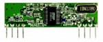 LCD display
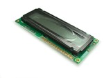
UNDER CONSTRUCTION
vk3pe
created on 15th July, 2008