

Last updated on January 17, 2024
My main web page
| The T41-EP Transceiver |
The T41-EP is a project by Jack, W8TEE and Al, AC8GY. Jack and Al designed an HF rig using the TEENSY4.1 Micro which is fast and suitable for the DSP software needed in the project. Display is a nice hi res TFT of 5". (Non touch screen). T41 stands for 'TEENSY 4.1", the -EP is "Experimental Platform" as the radio has been designed in modules to allow experimental changes. It's an Open Source project. There's a YouTube video on the project by Jack and Al here. Jack and Al published a book, "Software Defined Radio Transceiver, Theory and Construction of the T41-EP Amateur Radio SDT", (ISBN 9798446384240) which contains the theory behind a DSP based Amateur transceiver. Plus some information on the practical side of the project. The book is available on Amazon and is delivered very quickly as its an 'on demand' print service. The Book can be found here on Amazon. note BEST TO CHECK ON THE T41 GROUP TO SEE WHEN LATEST VERSION BOOK IS RELEASED. Further information on the project including pictures and Figures from the book, in better resolution, can be found in the Groups.io Group "SoftwareControlledHamRadio" Group files etc are found here. Please be aware even though Jack and Al's design is stated to be 'low cost', it depends on your "definition" of low cost. I live in Australia and our exchange rate with US$ means that we pay about 50% more in AUD$ than US$. The original costing's were in the region of US$250 I understand. (Update, it seems this figure is a bit on the loose side as the writer already had available, some of the high cost items.) I think it will be every bit of that and more. One factor in this is shipping costs. If you buy from various sources, each will have a shipping cost. PCB's have a shipping cost which can be quite high. eg I had 5 different PCB's made and shipping was US$35 which equates to $7 per PCB. (Ouch) I also ordered the other PCB's required in a Group buy on the SoftwareControlledHamRadio Group and shipping will be at least $10-12... all US$. The Teensy and associated modules are relatively expensive also, and the colour display, even more so! I dare not add up the totals for this project.........BUT....... I did a rough count...... and was amazed to find I have spent about AUD$450 on this project SO FAR. Ouch. And nothing like finished. Big dollar items are the Teensy 4.1, the AF module and display. If you are thinking to build this project, do a tally up of parts before you jump in, if a budget has to be followed. Keep in mind that resale values of home built equaipment is usually quite low. If like me, you love building gear, then it's not a big issue. |
|
I must admit that building is more fun to me than understanding the theory behind DSP, so this web page is more practical in nature and won't mention the theory.
I ordered only a set of the PCB's myself but have also embarked on making some of the PCB's myself, to use parts I have or just because I like to do it ! See below. June 2023, K9HZ is doing a different version of the 20W PA and will be selling PCB's and possibly kits or part kits also.
|
|
|
Jan 2024 Time flies and not a lot done on the project. I do have it receiving signals using my own Rx and Main boards. BUT:- Oliver, KI3P (formerly KO4THB), converted the new RF board (combines Rx and Tx sections) by Al, to the Kicad Sch & PCB editor software, from Diptrace used by Al. I have never used Kicad myself but decided to install V7 of Kicad to try and add some extra mounting holes in the combined RF board and Main boards to better suit horizontal mounting in the case I am using. It also brings those sections of the project up to date, using the latest schematics. This went without hitch, as far as I know, so I ordered both boards on 17th Jan and should have them around 25th Jan '24. Since I ordered the PCB's though, Oliver changed two parts on the RF board, to SOIC footprint from the smaller TSSOP footprint. Since I have the 74CBTLV3253PW parts in TSSOP in stock, it doesn't matter that I am using the old design.
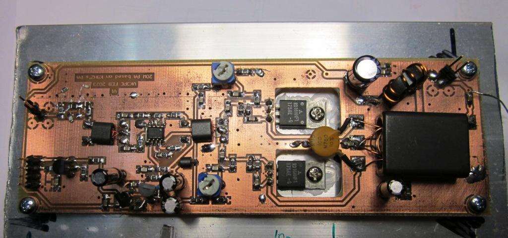
MARCH 2023 update Bill, K9HZ, has available his version of a 20Watt PA board using RD16HHF1 devices to replace the original PA. Bill plans to sell some of these PCB's around this time in late March. Bill is also working on a 100W PA using RD100HHF1 devices. I made my own version of this 20W PCB at home in Jan. and have been testing it recently. It's similar to Bill's version. A 2 week spell in hospital though, meant I have done little this month on it. It is producing stable output power. This my DIY version of the PCB: Not pretty but functional.
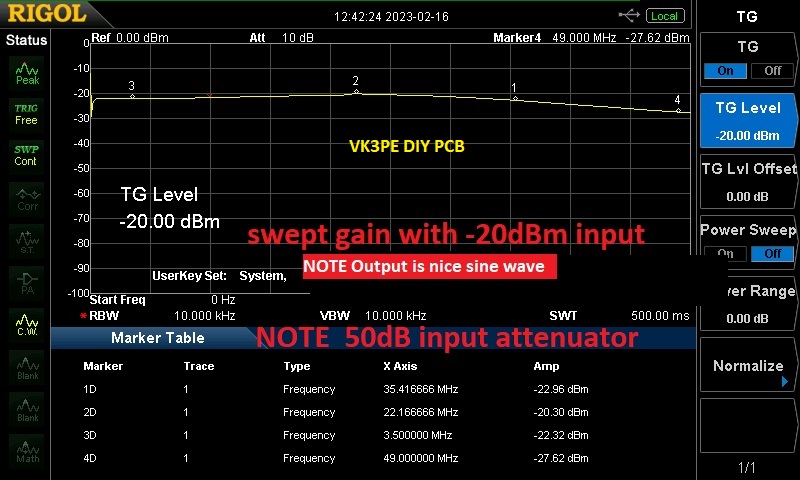
This is a sweep of my 20W PA at -20dBm input level.
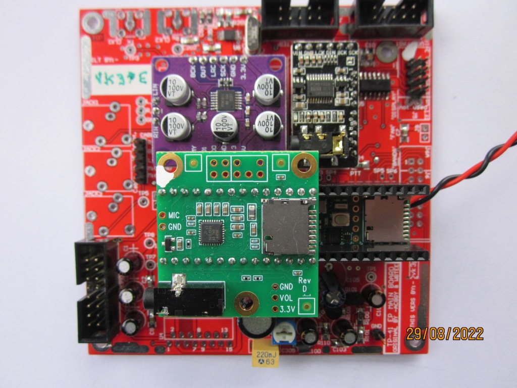
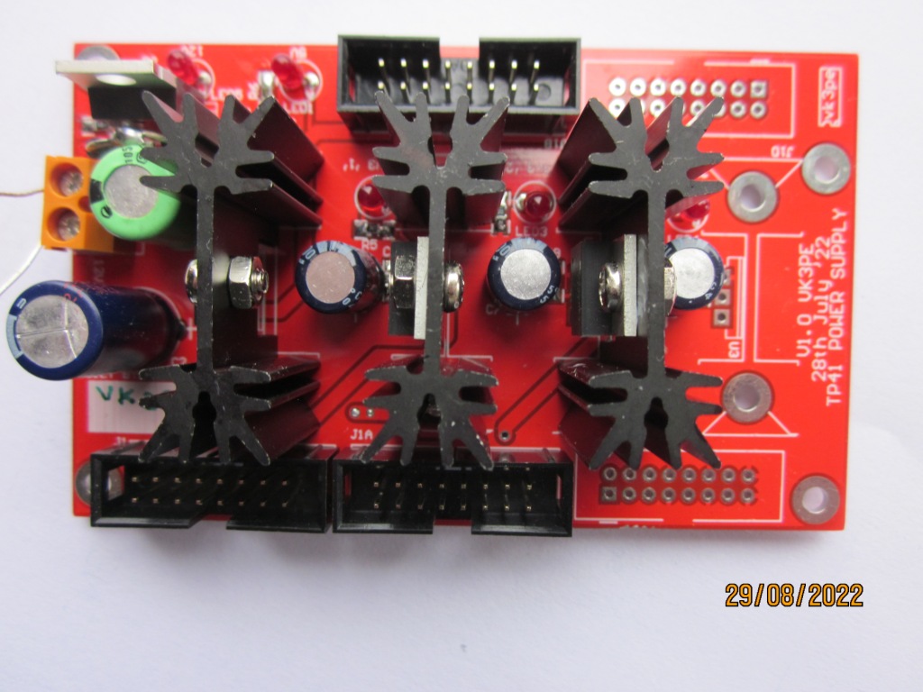
I understand others in the Group have been looking at a MC1496 version of the Exciter and also a single PCB for the existing Exciter and Receiver boards. Aug 29th 2022 UPDATE I received the 5 different PCB's I ordered and have assembled the Main and Power Supply boards. Bearing in mind the cost of these parts, I proceded slowly in powering up for the fist time. One at a time, etc. My PCBs are all red to differentiate myself from the group buy boards in the group. Power supply works fine. Main board appears to be working. I now have the display connected and its doing what I believe is correct, splash screen followed by the 'operating' screen. So far so good. One has to follow the instructions in the Group to initialize the EEPROM or it will keep reverting back to the the splash screen after displaying the normal screen, and so on. ie keeps resetting. Some hardware issues on original boards are detailed on the group also. One item not mentioned up to this point is the the real time clock (RTC) does not remember the time ! You have to fit a backup battery (CR2032 coin cell) in order to fix this issue. I will show this mod soon. I found a suitable case in my junk pile, an ex commercial test instrument. It's a little narrower than Jacks build above but should work out OK. I have made an aluminium front panel for it so far.
|
| July 13th - 31st, 2022 |
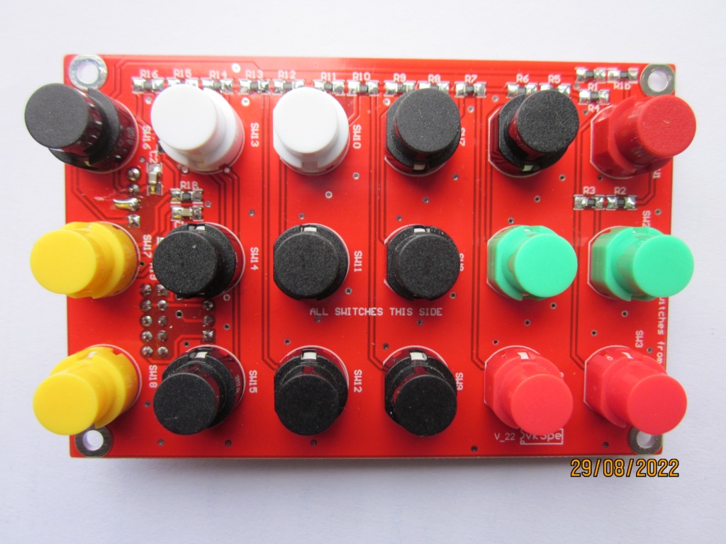
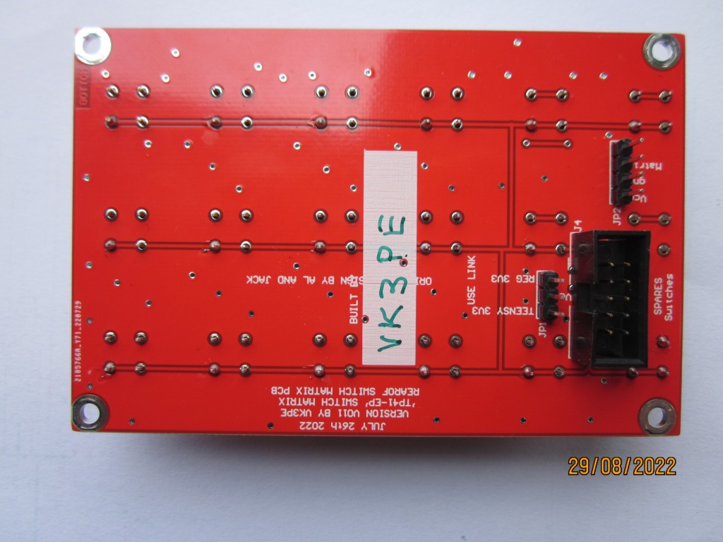
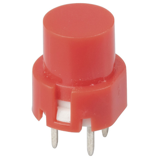
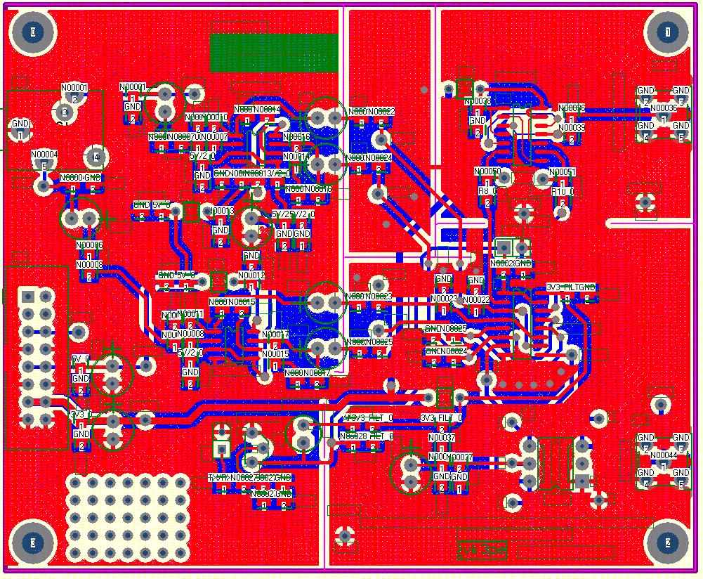
The original PCB designs were done by Al, AC8GY, using Dip trace. I am not familiar with this program so use what I have been using for a number of years. To design a PCB one normally starts with the Schematic, then uses the Net list generated from it, to make the PCB which is what I do. Schematic is also used to produce a Bill Of Material. I MADE SOME CHANGES FROM ORIGINAL TO SUIT PARTS AT HAND. eg. I used through hole transistors and FET's, also through hole Electro caps. Plus some other minor 'tweaks'. And in some cases, additions/corrections that were bought up by the Group. This takes a lot of time of course to re-draw them, but I have now completed the following Schematics, (and PCB's) based on V010 or V011, with a few 'tweaks' also. In late July 2022, I sent the gerber's out to get made. Hopefully have them back soon, about 2nd week in Sept. UPDATE Late Aug, they have arrived as above. NOTE: these PCB files and schematics etc are NOT officially endorsed ! T41 Main board contains the TEENSY4.1© 'control' module, Si5351© clock generator, plus ADC and DAC modules. Also, the Teensy AF module is used. T41 Main PCB schematic, and Sheet 2 There are some differences to original board to suit parts I have available. I added an optional provision to fit a TCXO for better frequency stability and accuracy. T41 Switch Matrix schematic. It contains 16 tactile push button momentary switches which are assigned various tasks. eg Band up, Band Down, etc. See picture above for details. Switches I used are round to simplify front panel drilling. (The original project uses square switches and the panel is 3D printed.) ie I am NOT using the push button tactile switches specified in the original design. I am using a locally sourced part available in four colours at ~ AUD$1.30. (from www.jaycar.com.au) They are also round components making it much simpler to drill the front panel for them. (square types were used in the original)
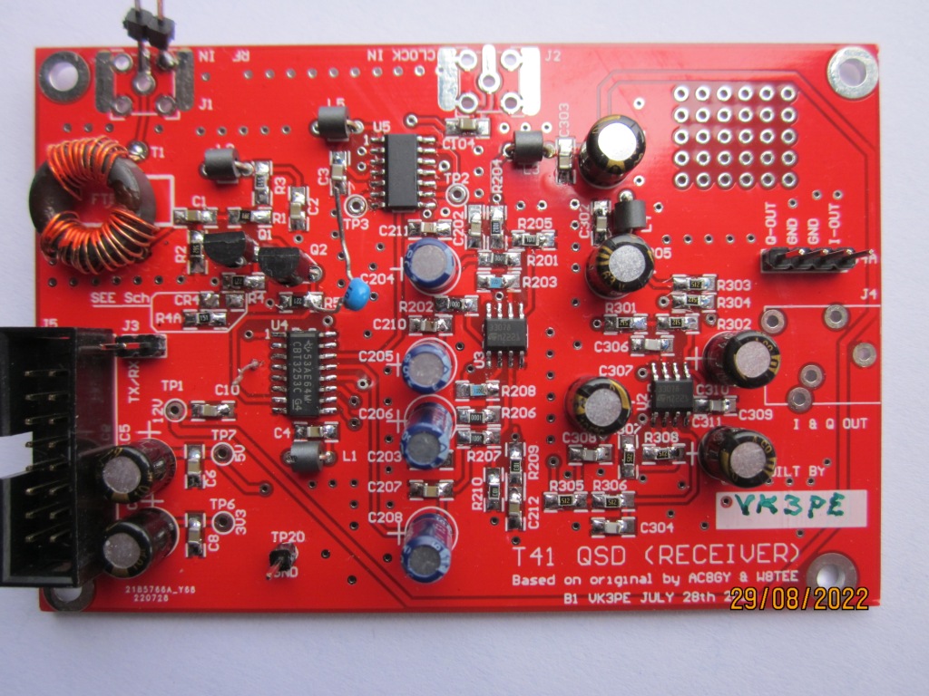
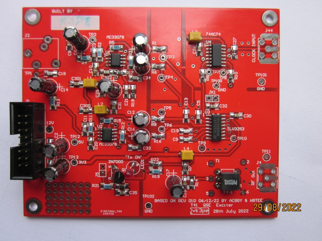
T41 Exciter QSE board schematic, ie Transmitter low level board. T41 Receiver QSD board schematic. ie the Rx front end excluding filters. I have added 2 parts in the RF Pre-amp stage to assist in leveling the response, if required. More later on this. T41 Receiver QSD screen copy. SOON. T41 Power supply board schematic. I altered the power supply board so it now has 3 x 3.3Volt regulators, to spread the heat dissipation and multiple IDC connectors for power out. Apparently the DISPLAY only, draws about 400Ma on 3.3v supply. Perhaps I should have added another 5V regulator also as I think that maybe it has the most dissipation?.(NO). I did add though provision, just in case, to put in a power resistor before the 5V regulator, to spread heat load if it looks desirable. T41 Power supply screen shot.
The above were drawn by me using the original V010 or V011 schematics, so may contain errors. There are some errata in some original documents and PCB's and these are detailed in the 'Errata' section of the Groups Files area. PARTS: There are BOM's (Bill of Materials) for each of the boards and some group members have also created BOM with part numbers from Digikey and other suppliers. These are USA based though so don't really apply to Australian builders unless one can accept the relatively high shipping charges. In the main I plan to use parts on hand or those available from Element14/Farnell®. The TEENSY 4.1 and it's associated Audio board can be found on-line as can the PCM1808 and PCM5102 modules. Eventually, I will add the BOM for the 5 PCB's I designed also. Obviously they will be similar to the originals except for the components that I used from my own sources. My BOM will not contain any Mouser, Digikey etc part numbers as I don't buy from them unless absolutely required, mainly due to shipping costs. The 5" colour display is sourced from BUYDISPLAY.COM and details of exact type can be found in the Group. Larger 7" and 9" can also be used but will need careful thought to fit to a case.
OTHER VARIATIONS: Most probably I will be using a G6ALU design 140W PA and a G3TZR Low Pass Filter. For the receiver side I plan to use band pass filters, not the LPF's used in the original. I also have a available a commercial BARRETT 100W PA with in built low pass filters which could be used. TESTING: Jack and Al have recently uploaded a "how to build" document on the Group site .I will check it out when I start to assemble PCB's. I have done some basic testing of my own though on several boards so far.
ASSEMBLY INTO A CASE: The original project was built into a 3D printed front panel and case. I have no access to 3D printing so will re-purpose an old instrument case I have. It's a little narrower and deeper, but is a low cost way to build it, for me. It's actually an identical case to what I built one of my PIC-a-STAR transceivers into. You can see it on my QRZ.COM page, top right corner. Still to do, drill holes for the various controls and encoders:- Lettering of the panel will probably be done by colour printing a large sheet of paper then gluing it on. and a clear coat over that.
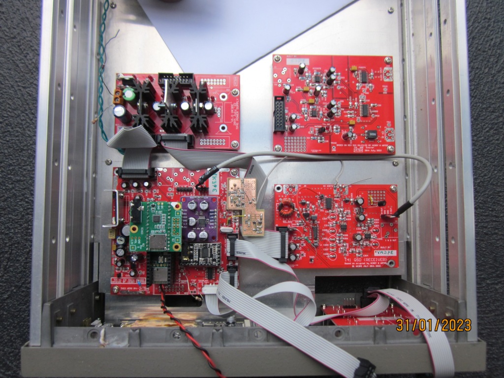
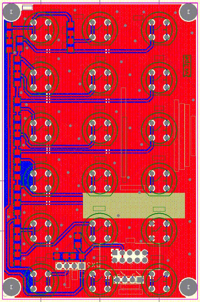
All of my PCB's were designed to mount "flat" in the case, for easier access for testing etc. Shown below, power supply, Main board, exciter and receiver PCB's. The flat IDC cables will run to the Encoders on front panel, once I decide on exact layout.
The small home-made PCB in the centre is a buffer board to bring the Si5351 output levels up to about +7dBm or so.
This web page was created by VK3PE on 13th July 2022 (email on QRZ.COM) No guarantees are given or implied as to the suitability of this material for any purpose whatsoever. Information herein is presented for amusement or entertainment only. Any inadvertent use of Trademarks is accidental and not an endorsement or otherwise of a product. I have no commercial link of any kind to suppliers or brands mentioned here. This page will constantly be under construction, come back again !
|
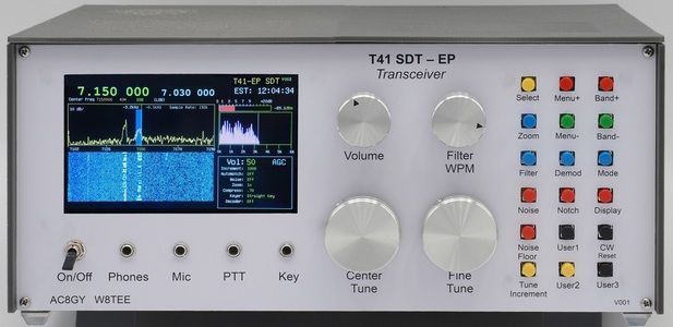 Jack and Als version.
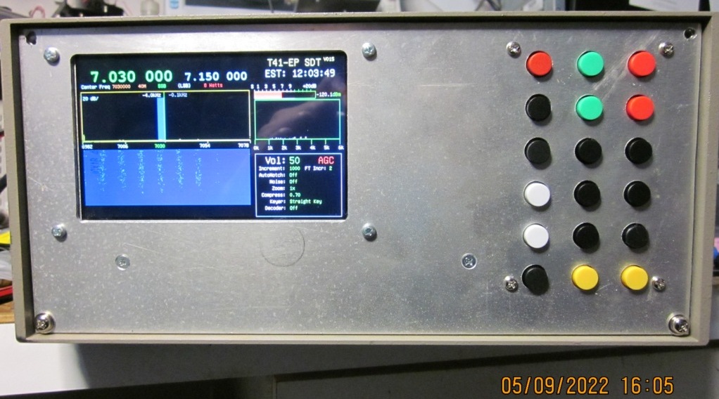