DSP Opto Isolator PCB
This is my own implementation of the suggested Isolator for PICASTAR DSP motherboard.
See it here. (schematic)
On the schematic: NF = Not Fitted, a better value for the 2k2 is 1k.
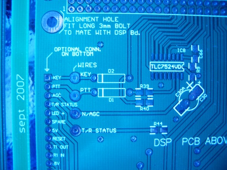
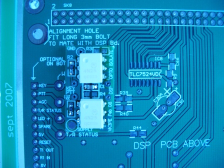
I made a small PCB that fits over the D1 & D2 diode area of the VK3PE pcb's. It's a sample PCB.
If I do make more, it will be in a corner of the planned BPF pcb. I cannot make it seperately as cost would be high for small numbers.
(Update: This PCB was part of the Panel #2)
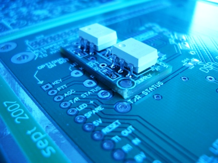
I used 4N25 opto isolators. This PCB was NOT designed for the optimum isolation that the part is designed for !
It does allow easy fitment to the vk3pe PCB'.
The diodes (D1, D2) are removed and wires inserted into the diode holes then the PCB is fitted over the wires. A GND hole needs a wire also. Then 5v (or 8v) needs to be bought to the PCB from the bottom left pad on the PCB (wires are not shown here.)
A pcb with top layer only . (foil for PCB)
This NOT the PCB shown above.( It was 2 layers)
vk3pe
November 12, 2008