A HOME-BUILT
"HF Transceiver", BASED ON THE BOOK BY EI9GQ
Dec 2020, BOM and Sch added for the "QUAD" pcb's shown below and also a version of EI9GQ's 16W PA.
April 15th 2019:- HYCAS PCB now loaded
March/April 2019 an alternate BPF using solid state switching ie no relays.
January 28, 2019 Another web page for a 40M rig I might build.
January 26, 2019...... A new PCB for the '16W' amp and other new Boards added..
Previous update:-
A VFO based on the uBITX's Raduino board.
16Watt PA stage built and 3 stages tested and home brew crystal filter
June 23rd New PCB's built, that combine some functions.
MC1496
based balanced modulator Sch added.
PREFACE
The project on this page is of an HF Amateur band Transceiver built around the information in the book "Building a Transceiver" by EI9GQ & G4LFM. Some variations have been made in my build to suit parts to hand or to replace parts not easily obtainable.
This web page is presented in "Chapter" form as per the book. Some additional information on my build and PCB's etc is also presented at the end of the EI9GQ book.
See here for VK3HN's review of the EI9GQ book and also, for VK3HN's build of this project. You might even spot me in there!
INTRODUCTION
After building a number of HF Amateur radio rigs,
including a several (7 !) Picastars, I was looking for a new project to use
some crystal filters found on eBay that were given to me. The filters are KVN
branded and are part of some sort of SSB device, the PCB is made by Telrad™,
perhaps not an actual HF rig. The filters were removed and also the MC1496 IC's
(3) on the PCB. Not much else of value. There are three filters on the PCB;
USB, LSB and AM filters. Only the USB & LSB will be used in the project.
Click on most pictures for larger
view.
 What started this build, some SSB crystal filters available on eBay.
The inspiration for the build is a book by Eamon
Skelton, EI9GQ, who writes a column in the RSGB Radcom© magazine. I am not a member of the RSGB, so I am
unsure if Eamon still does the column, but the book appears to be a compilation
of those ideas that do not appear on his own web pages. Eamon used axial components,
without any PCB's. I elected to use SMD parts where suitable on my own design
PCB's.
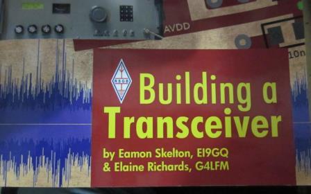 This is a partial picture of the front cover. The book was printed in 2014 &
2015. ISBN: 9781 9101 9301 3 (I have no
personal or commercial connection to the book or author, except for its purchase.) The book
is not very expensive and a great read, even if just for some ideas. I imagine
it's available via the RSGB or in some countries, from technical book sellers.
This is a partial picture of the front cover. The book was printed in 2014 &
2015. ISBN: 9781 9101 9301 3 (I have no
personal or commercial connection to the book or author, except for its purchase.) The book
is not very expensive and a great read, even if just for some ideas. I imagine
it's available via the RSGB or in some countries, from technical book sellers.
My project relies heavily on Eamon's book but with
some changes to suit parts at hand and also in some cases, to make the modules
50ohms in and out. All PCB designs are either 50x50mm or 50x100mm in size.
Since the book is Copyright©, I won't publish the
Schematics here, unless I can get permission to do so, or they are my own variations.
But, I will show the modules I have built so far in the project. All modules
were drawn up in Schematic form, then a PCB design made for them. So far I have
made enough modules to get the Receiver running. The transmit modules have mostly been built. For the VFO, I used the Si5351
device which is very popular, although not an ideal choice in a hi-performance
rig. Later, I think I will move to the AD9951 DDS chip as I have made a PCB
for it and have the chip in the junk box, from Picastar builds.
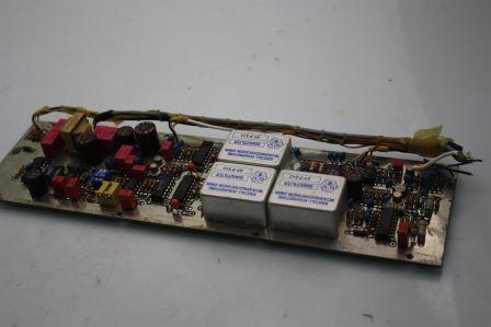
Below, is a picture of MY HOME-MADE pcb's forming the receiver side of things.
The audio amp uses a different device (bottom left module) but otherwise is
much the same as Eamon's except for variations as shown above. The crystal filter
board and Rx band pass filters (see below) are shared between Rx and Tx modes.
 To the left, are the receiver sections. The VFO and display is not shown. Top
left is Rx mixer and post-mixer amp, then crystal filters, bottom right is the
IF board and AGC boards, then the demodulator and audio. (Clockwise from top
left) Bottom (angled) is the 9MHz crystal oscillator board.
To the left, are the receiver sections. The VFO and display is not shown. Top
left is Rx mixer and post-mixer amp, then crystal filters, bottom right is the
IF board and AGC boards, then the demodulator and audio. (Clockwise from top
left) Bottom (angled) is the 9MHz crystal oscillator board.
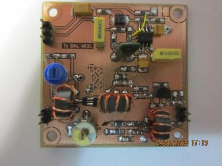
Chapter 1, Balanced modulator:
I didn't build the "SSB exciter" as I will be generating the VFO and BFO signals using an Si5351. In this chapter though is the Balanced modulator. I built the diode version and also an LM1496 version to compare. I like the diode version better as less parts and I think better carrier supression.
THE TRANSMIT SIDE:
Balanced Modulator will be either
classic MC1496 based, or use a diode DBM. I have built up both types and will decide
which one to use, after testing. Eamon didn't use the MC1496. In the diode Balanced
Modulator I used two BAT54S diodes which is a dual diode in a SOT-23 smd case.
 and the 'pro' made version.>>
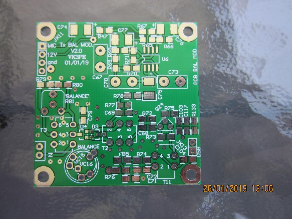
Diode Balanced Modulator Schematic and overlay (coming)
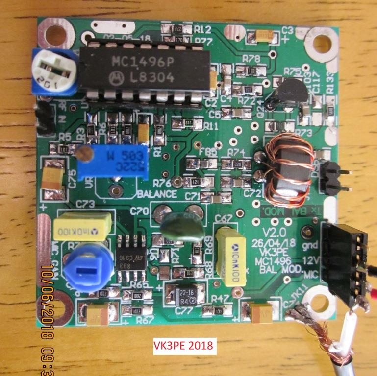 MC1496
Bal Mod. Schematic. As you can see, many more parts required.
MC1496
Bal Mod. Schematic. As you can see, many more parts required.
MC1496 BASED BALANCED MODULATOR, Schematic. Based on the MC1496 Data sheet, plus a Microphone amplifier stage.
Either board above produces double side-band (ie DSB with supressed carrier),
so, to get SSB, we need to remove one sideband. This is done by using the crystal
filter, shared with the receiver. A post mixer amplifier brings the level up
for application to the Tx Mixer.
Chapter 2: Transmit Mixer and band pass filters (BPF)
Tx
Mixer.
This is the Transmit Mixer board. It takes in SSB
generated by the balanced modulator and crystal filter, the VFO and shifts the
output by mixer action, to the band of interest. Not fitted at right side, is
the actual mixer, a double balanced diode type JMS-1 from the junk box. Board
was undergoing tests here. It's followed by the Rx BPF, switched in to the Tx
side, to remove unwanted products.
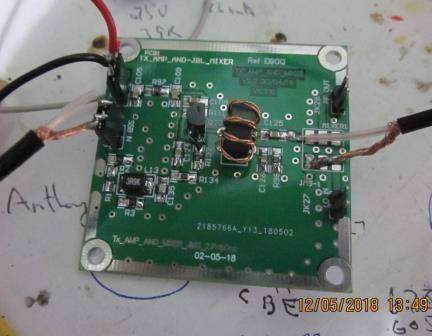 Tx Mixer (actual mixer not fitted)
Following the Tx mixer & BPF, is the post mixer
amplifier stage: See further down.
CHAPTER 3: The BPF & low level transmit amplifiers stages.
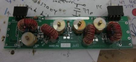
Band Pass Filters. Only one is shown here, for 80M. In my case I made them as plug-in modules to a mother board.
The band pass filters are switched between the Receiver and Transmitter sections.
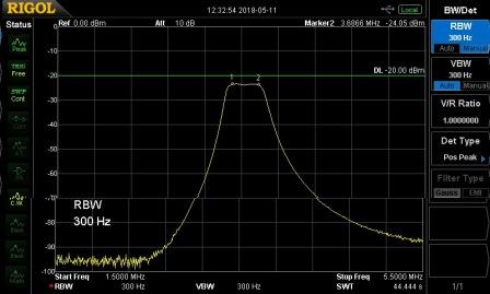
 This
is a plot of the 80M band pass filter (BPF) board. (Loss about 4dB in-band.) Each
band is a plug in module so I can fit as many bands as required. All BPF boards
are identical with on-board relays (not fitted in picture) for switching, loaded
with parts to suit the band required, of course. BPF Modules, Schematic and overlay (Refer to the book for values) See also further down page for the motherboard.
This
is a plot of the 80M band pass filter (BPF) board. (Loss about 4dB in-band.) Each
band is a plug in module so I can fit as many bands as required. All BPF boards
are identical with on-board relays (not fitted in picture) for switching, loaded
with parts to suit the band required, of course. BPF Modules, Schematic and overlay (Refer to the book for values) See also further down page for the motherboard.
An alternate BPF board?
Also, I have been thinking of making a simpler BPF board that uses solid state switching instead of relays. I found some interesting devices that are obtainable locally, the AS169-73 by Skyworks™. A PCB was drawn up in March 2019 and I am waiting for it to arrive. (see below) I have done some testing though beforehand and they are very good. I get in excess of 70dB isolation when the band is turned OFF on atest setup. Current requirements are extremely low. Just a few mA.The board uses the same devices to switch between Rx and Tx modes also. It would replace the BPF modules and motherboard shown here, if I go that way. Size of the PCB is 50x100mm. It's only for 4 bands, BUT the PCB's can be stacked for 8 bands if required. It's shown below, a screen shot of the PCB, not loaded. I also decided to try these switching devices in the Crystal Filter switching. More to come on that.
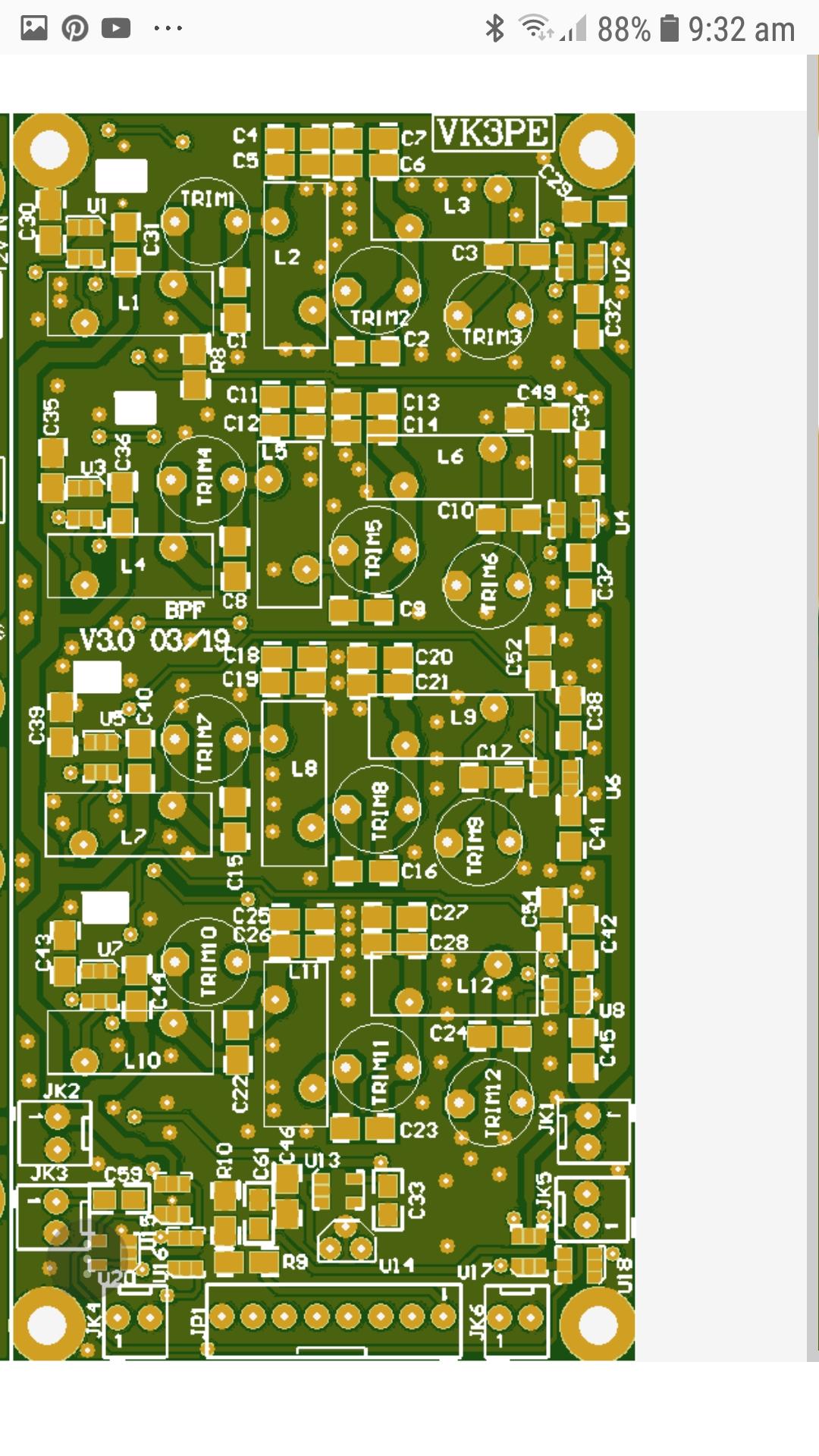
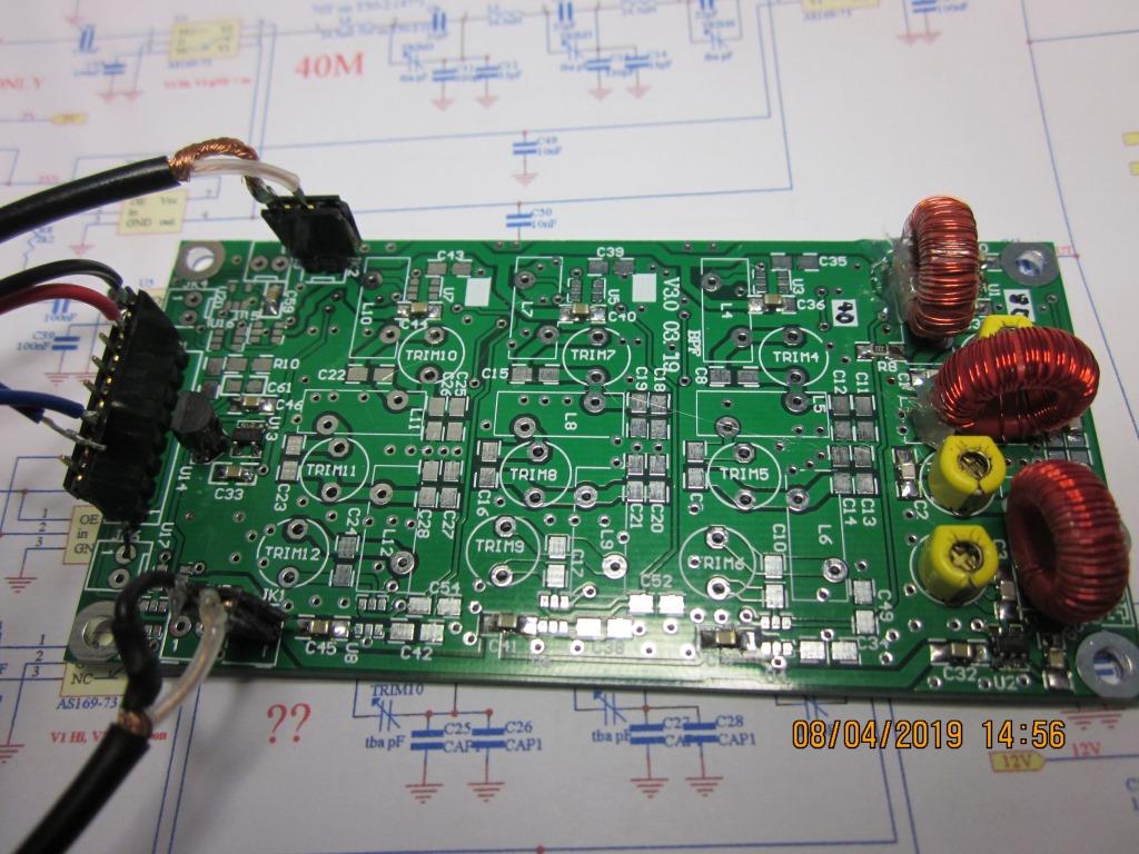
The BPF PCB above has now been received (Apr 2019) and partially loaded with the 80M band components (toroids are T50-2) and switching components. Results look very good! Even better than expected actually.
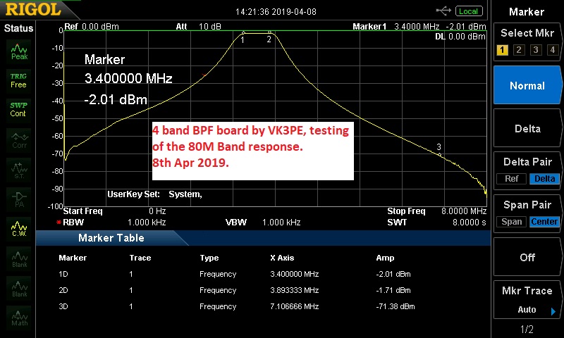
Here is a plot of the 80M band shown above, which actually came up almost without needing any tuning. Just a very slight fiddle was required with the trim-caps. The BPF itself is based on the Picastar BPF but using toroids in place of TOKO coils. In-band loss of less than 2dB is much better than the Picastar (4-5dB), due no doubt, to the higher Q of the Toroids. When switched out of circuit, noise floor is >90dB. This low loss will be better when switched into the Tx side also.
Next I will fit the 40 & 20M components. Not sure about band 4 at this stage.
 Click for larger picture.
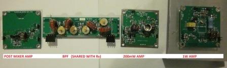
Low Level Transmit amplifiers:
There are two stages of RF amplifiers following the BPF when in Tx mode. These amplify the low level SSB signal to bring it up to a suitable power level. The modules built so far bring
the level up to 1 watt.
You can see the whole Tx chain here,
from the Tx post-Mixer amp, right through to the 1 Watt stage.
 click for bigger picture.
Following the BPF, the Tx low level amplifier brings
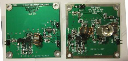
the signal up to around 200mW.
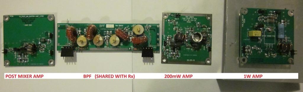
Shown below are the post Mixer buffer amp (left)
and the 200mW stage which follows the BPF. It uses a 2N5109 in the second stage
with small heat sink. It drives the next stage a 1Watt amp. shown further down
this page.
 SEE ALSO BELOW for testing of the RF boards; 31st Oct 2018
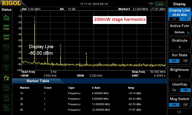
In testing alone, the 200mW stage was found to have
predicted gain and is very flat. Input required is about -19dBm. Harmonic suppression
also good, as can be seen below.
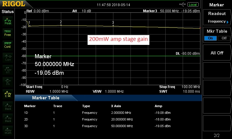 Response is 'Flat' to within 1dB from 2 - 50MHz
Next stage in the Tx side is the Tx PA driver stage
which ups the level to around 1 Watt. Eamons original used an RD06HHF1™ but lacking
one of these, I fitted the higher power RD16HHF1™ device. It still puts out about
1 watt in this schematic, as tested. Following these stages will be the "16W" amplifier based on 2 x RD16HHF1's in push-pull. I don't have concrete plans as yet for the
PA finals but possibly something based on the G6ALU 100Watt amp might be used,
as I have used it in Picastar. Then a low pass filter of course according to the band.
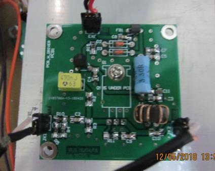 The RD16HHF1 FET is mounted under the PCB and bolted to a heat sink.
No doubt many of the modules could be combined to
obtain an overall smaller set of PCB's. SEE BELOW !! The present method
allows various sections to be change easily though. Perhaps later, I might do
something to make the rig PCB's smaller overall. Right now though the intended
case for the project has plenty of room so it's not urgent !
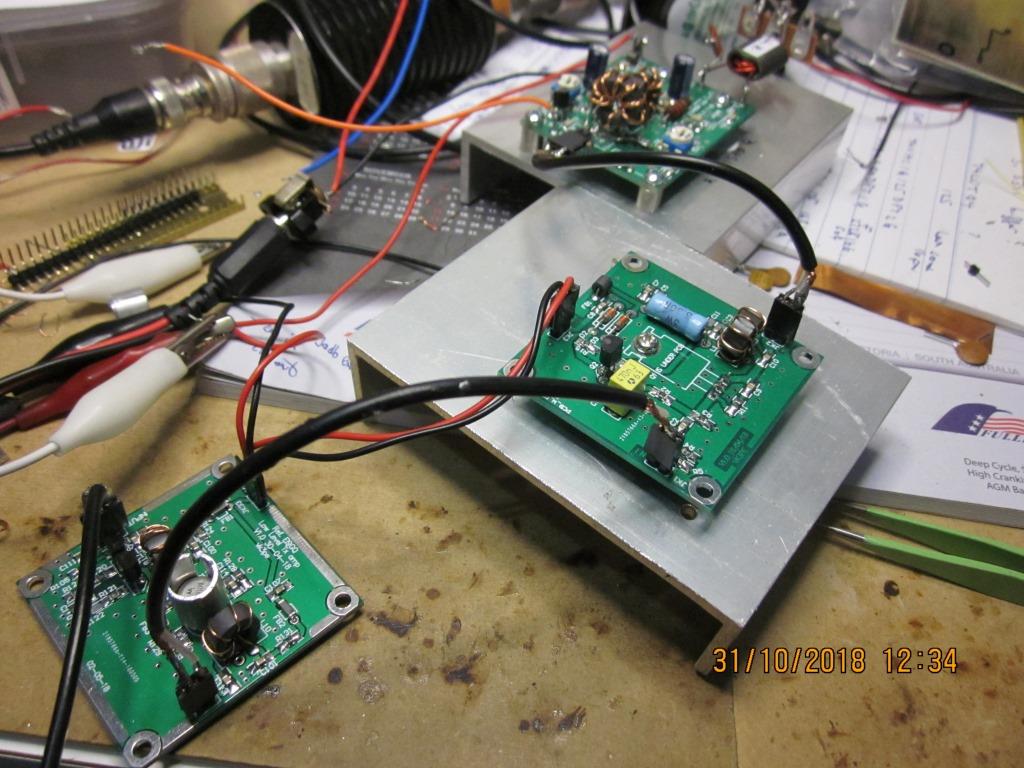
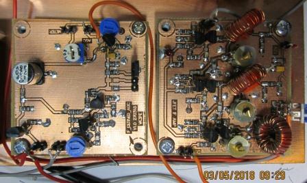
UPDATE: 31st Oct 2018 (Halloween)
I have now tested the three Tx RF boards together. ie the 200mW, 1W and 10W boards, connected together and fed with a signal etc.
The stages are:-
200mW: 2xMPSH10's in parallel, driving a 2N5109 (or similar) in class A.
1W: RD16HHF1 in class A (specified is the RD06HHF1 but I didn't have one)
10W: 2 x RD16HHF1's in push pull. NOTE: the output transformer is now a Balun core rather than the two toroids wound with co-ax. The two input toroids also replaced with a single toroid.
Excuse the messy bench but the three boards are there if you look closely !
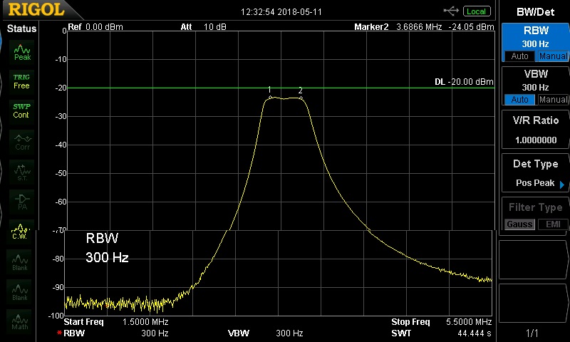
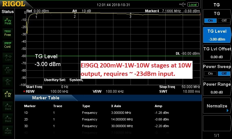
I get over 10W output with ~-23dBm drive level from sig gen. I also swept the setup at the same input level as you can see below. The response is extremely 'flat', within +-1dB. Amazing actually I think. And very useful right into the 6M band too.
 This is not my current 16W board, but the version with incorrect output transformers. See the NEXT Chapter.
And the input VSWR is excellent also.
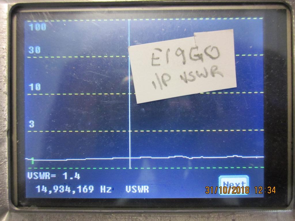
Very pleased with the Tx RF amp stages so far.
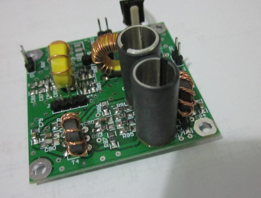
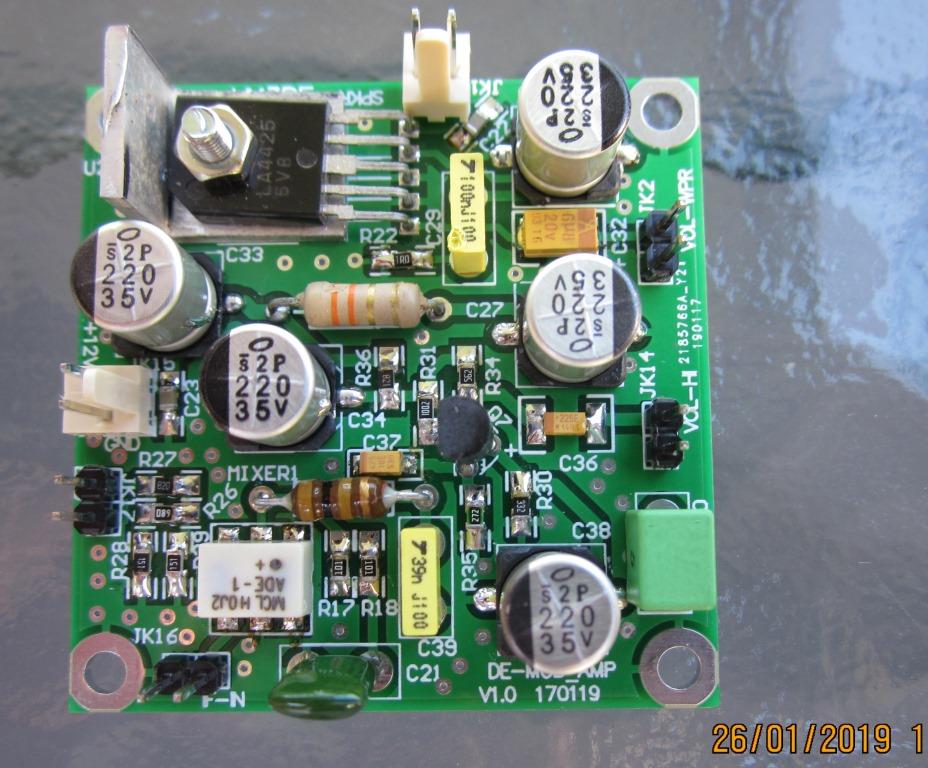
CHAPTERs 4 & 5, Broadband Linear Power Amplifier
The PA Stage
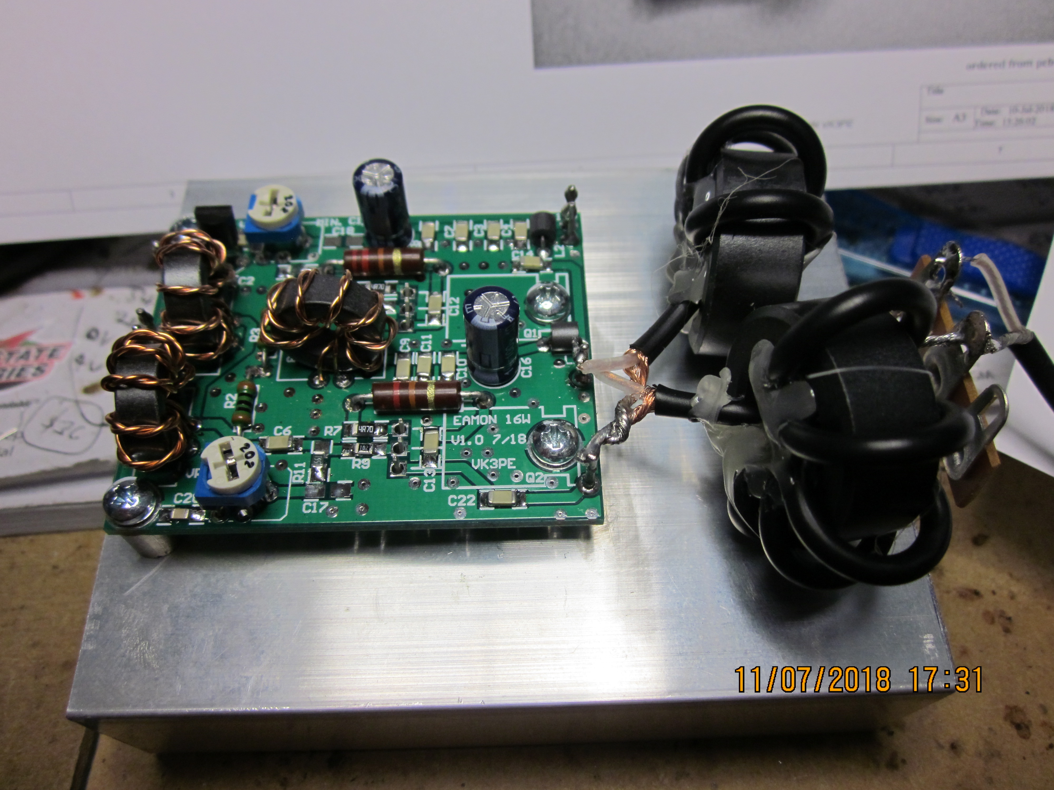
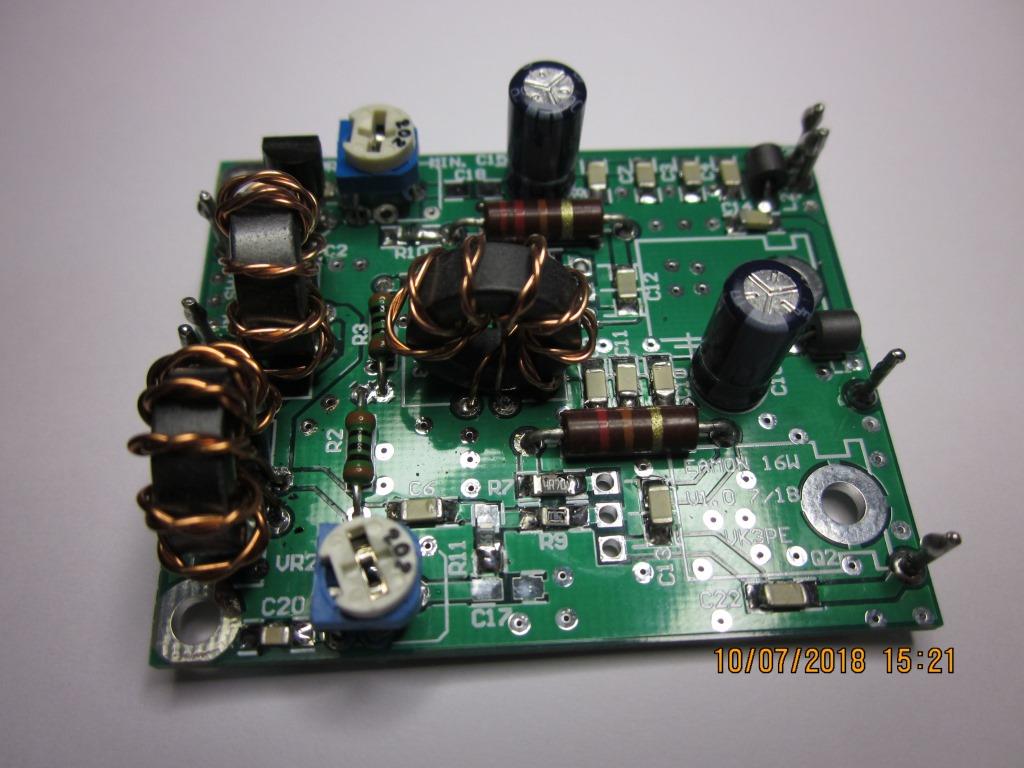
EI9GQ has details of several PA's the 16Watt and also some much higher power levels. My initial needs are for the 16Watt stage so a PCB was drawn up quickly to take advantage of a free shipping, Chinese supplier deal. The PCB had to be under 2500sq mm so a board 45x55mm was designed. This is way too small of course for the complete Amplifier but I took advantage of the deal with the smaller pcb size and an 'outboard' final transformer stage.
Eamon used some toroids in the final stage that are not available in VK. Nor perhaps, in the UK as the supplier, Maplin, has ceased trading. I used some toroids of near identical size (25mmOD) but available locally from www.Jaycar.com.au (LO1234) who have a nearby store. I don't know what the ferrite type is ("L8") but since I had some of the toroids i used them. The original design calls for 25 ohm coax to be wound on the toroids. Eamon used some single core audio shielded cable which he had measured to be about 25 ohms impedance. Not ideal co-ax of course. I had none of this cable on hand so used standard RG174 50ohm coax instead with the same 6 turns.
I did make a few changes to the original schematic, adding some ferrite beads for the input supply, additional bypass capacitors, plus electrolytic caps on the supply also. I also added small value (4.7ohms) in series with each gate.
Surprisingly, I powered it up and it works. Right now I am only driving it with 0dBm signal for testing but the gain curve is very similar to that obtained by EI9GQ but where he got about 11dB gain, I am getting a few dB more. The real test will be feeding it with more input power, 500mW to 1Watt from the stage built above, should be just fine.
Here are some pictures of my PCB and the final amp. It uses RD16HHF1 FET's mounted under the PCB and heat sink to the chassis. (click picture for larger size)
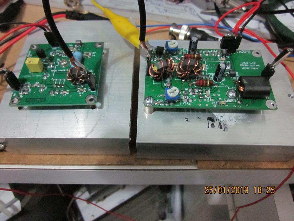
Jan 2019:- PA Updated, new PCB
I decided to alter the PA board above to my own version, with the changed input and output transformers. Instead of using the two input baluns to form a 4:1 transformation, I simply wound a FT50-43 toroid to do the same job. It was wound in trifilar and carefully phased so 2 of the windings in series, form the primary or input side. The other winding becomes the output, into the FET's.
For the output I went with a BN43-202 core, wound as 2:4 turns. This may not be optimum but serves as a starting point.
I will place the Schematic here, as it is my own variation of EI9GQ's. Coming soon.
I ordered a new PCB from China and it has now arrived. See test results below.
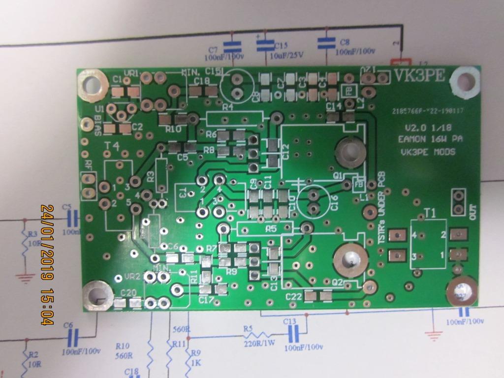 NEW PCB.
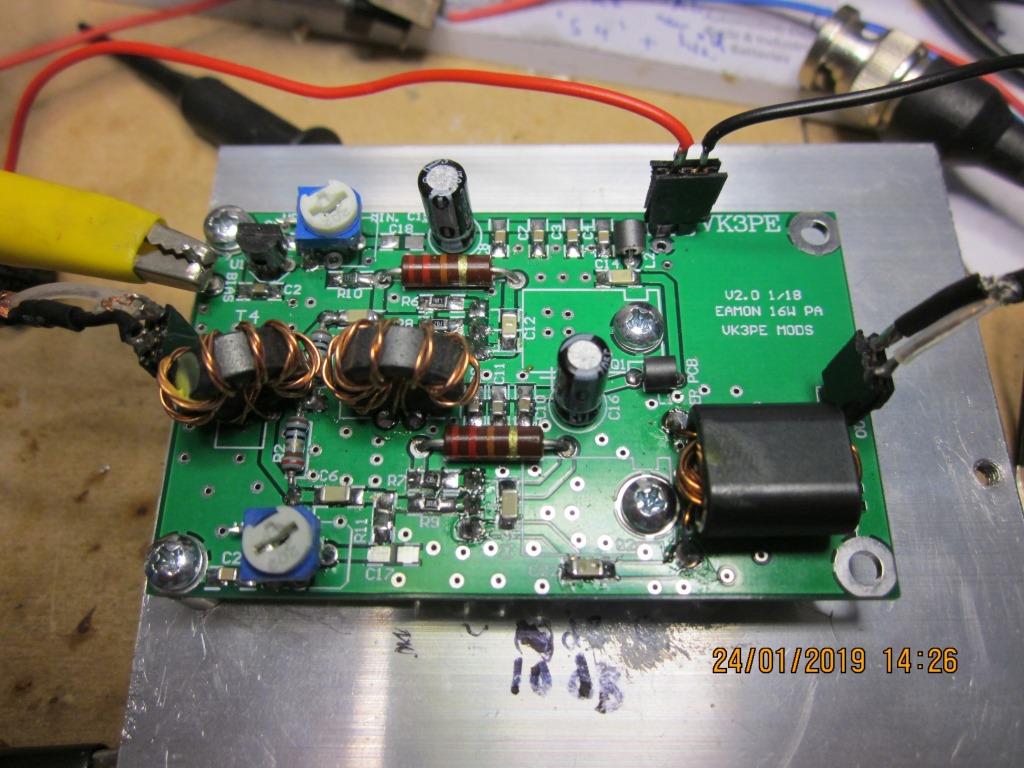
 NEW version.
 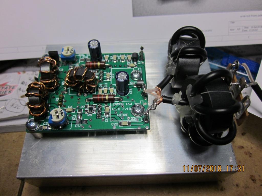 OLD version.
My build is biased at 250mA per device here, EI9GQ recommends 500mA per device.
The loaded PCB. Undergoing testing by sweeping it on it's own, at 0dBm input (max. from SA with tracking gen.)
Sch and BOM of PCB in picture below: New Dec 2020
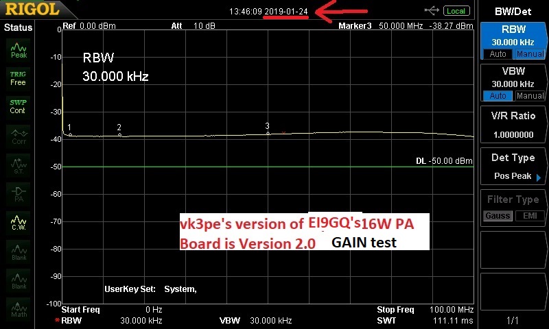
And the frequency response and gain. The green line is "0dB" gain or reference. As you can see, the gain is almost constant at 12dB up to around 80MHz. Slightly less than my original build but possibly due to output transformer not being optimum ratio. Still sufficient though to give 10W out in the Tx line-up, I believe.
 NEW PCB.
Power output test. I fitted the 1W stage as shown on this page, as the input stage and drove it with the HP8640B sig. gen. Max. output running at 12.5V was approx 12.5W. I settled for 10W out and will set the drive for this level when the whole Tx is built up.
CHAPTER 6 Starting the Receiver section. Fig 40 & 42
Here is my un-loaded receiver mixer and post mixer amplifier. It differs from the book in that a packaged mixer is used. An ADE-1.
 The mixer is a DBM, type ADE-1™ or similar.
Jan 30th, 2019: Although not shown here, the above PCB has been partially assembled. Some tests were made of the diplexer which follows the actual mixer. (The PCB is designed with links so sections can be isolated for testing) It's function is to terminate the Mixer output over "all fequencies". So, I swept the diplexer and as you can see it's working well, a peak at 10,7MHz. Loss about 1dB exactly as predicted in the book. (The schematic is in the book, at Fig. 40.)
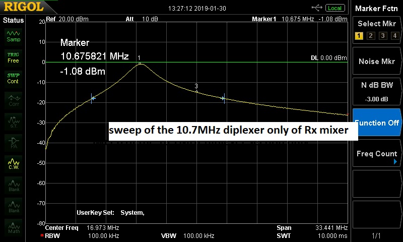 Frequency sweep of the Diplexer only.
The SWR was also measured with the output terminated with 50ohms. Again, all appears to be OK>
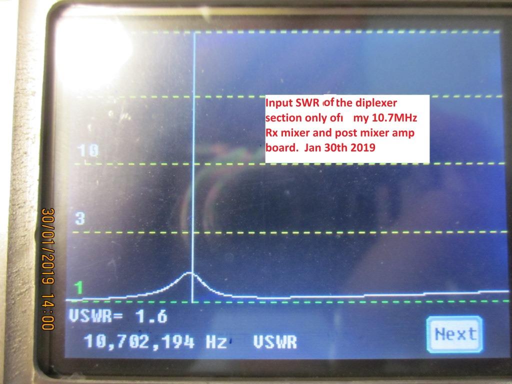 SWR of the diplexer only.
Here is the loaded PCB, while being tested. (the Mixer, an ADE-1, is not yet fitted):
The yellow toroids are part of the Diplexer.
The post Mixer Amplifier schematic is Fig 42: in the book, although it doesn't specify the number of trifilar turns on T1 & T2.
I elected to go with 7 turns on FT37-43 cores. This may have been a mistake on my part, as a quick frequency scan of the Post-Mixer Amp only, showed the gain at 10.7MHz = ~10dB but it rapidly falls off below about 9MHz. Maybe more turns are needed. Everything else on the PCB seems ok. Input SWR is OK though at < 1.4:1 from 3MHz and up. I will try some more turns on T1 & T2 ASAP. It's actually OK for intended use, but still needs to be investigated as the amp may be useful elsewhere.
A picture of the loaded PCB and more tests soon.
CHAPTER 7, IF Amplifier, product detector and an Audio Amp.
IF Amplifier / AGC
I used the schematic in Fig. 45 and for the AGC used Fig. 53, BUT I had to alter the AGC output stage by removing the FET and replacing it with an NPN transistor. The source resistor (4k7) was removed and placed in the Collector circuit, the collector now feeding the AGC output and S'meter.
The heart of the receiver is the IF strip. In my
build, I used the 3 stages of cascode JFET's rather than the MC1350 stages also in
the book. I blindly used the suggested AGC circuit but soon discovered it was designed
for the MC1350 stages, as the voltage sense was reversed. Some on-the-run changes
were made and can be seen in the AGC board (left). The FET was changed to a
transistor and the AGC voltage taken from the collector instead, with emitter
grounded. The AGC seems to work well in listening tests but no other tests have
been made yet. IF gain is around 68dB. UPDATE April 2019: there is a problem with my replacing the FET with a NPN device. Silly oversight. Input impedance is much lower so AGC contsnats are not correct. Working to correct this ASAP. OR use the HYCAS AGC ideas below.
NOTE:- the IF stages are very similar to that used in the "HYCAS IF Strip" although the AGC section is a bit simpler here. I understand that a PCB for this W7ZOE IF strip, is available. See below.
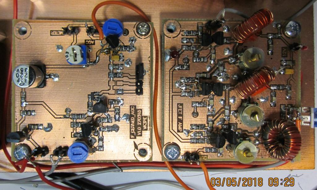
 Proto AGC and IF stages. BF256 FET's were used. The 4 pin connector
on the AGC board is to select AGC decay.
Proto AGC and IF stages. BF256 FET's were used. The 4 pin connector
on the AGC board is to select AGC decay.
The following material material is NOT in the book, but presented for interest:
The IF section is very similar to that published for the HYCAS IF strip by W7ZOI although the AGC Sch is different. Suggested reading is w7zoi.net/hycas-pcb.html See also below.
Here is my 'HYCAS' AGC board ready to be assembled. (see below) It would replace the PCB on the left, above, with slight mods to the IF amp to make it compatible.
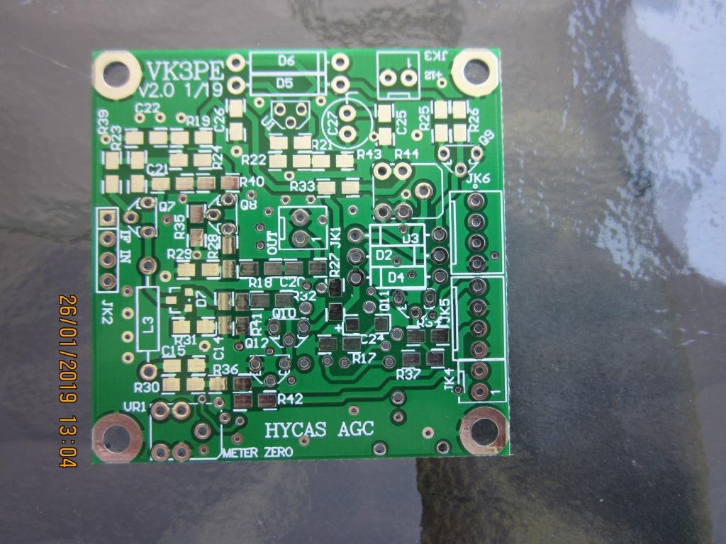
The PCB was received in early 2019 and has now been loaded although yet to be tested. That will occure once I build the HYCAS schematic version of my IF board.
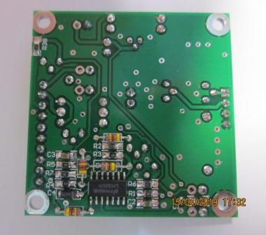
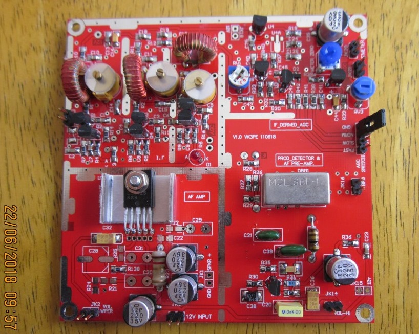
The Product detector and audio amplifier: Figs. 45, 46 & 47 My Schematic
The IF board then connects to the Product Detector, see below. It also has the audio pre-amp and power stages on it. The board is 50x50mm shown below. Note the actual power amp stage is different to EI9GQ's book. I used the LA4425 chip which is similar to the TDA2003 specified, but requires less parts around it. A scrap of aluminium is used as a heat sink. This chip is obsolete, but still available from various places. I used http://www.utsource.com On the larger 100x100mm Receiver board shown on this page, I also made provision to fit the TDA2003. Some other parts substitutes were made also, to suit parts to hand.
I used an ADE-1 mixer from Mini-circuits rather than make my own as per the book. It's at bottom left.
 NOTE: C37 polarity is not marked on the PCB.
CHAPTER 8, 9 and 10. Local Oscillators and DDS VFO:
For now, this chapter is skipped as I am using an Si5351 and an Arduino NANO.
Will advise on what I do, soon.
CHAPTER 11, band switching:
The Band Pass Filters were shown above. For switching bands I made a 'motherboard' that allows upto 7 BPF's to be fitted and relay switched.
March 2019:- See also the new section on an experimental BPF using solid state switching devices, above.
Only one is fitted in the picture,
the 80M band. There are two relays under the PCB which switch the BPF selected,
between the Rx and Tx stages. It will probably be fitted into it's own shielded
enclosure.
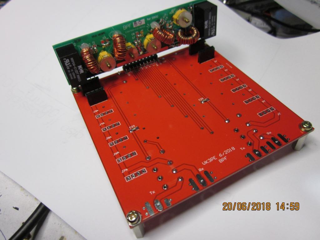
BPF Modules, Schematic and overlay (Refer to the book for values)
BPF Motherboard Schematic and overlay (Note ref to C5 and C6 on overlay)
CHAPTER 12 Broadband Driver amps. and generating CW.
For now I am sticking with the 10Watt only stage but later may fit a higher power PA by G6ALU. (Google G6ALU for information)
I have no current interest in CW, nor are there CW filters in this design, so have done nothing with that.
CHAPTER 13 and on.
I won't be using or building any items in these chapters although some is similar to that presented by G6ALU. (Google).
Other material of interest perhaps:
In some cases, as the build progressed, I had some
PCB modules made in China from my designs, as you can see above. e.g. the crystal filters on a new PCB compared
to above picture. It turns out to be cheaper sometimes to have them made in
China, compared to the cost of buying Kinsten™ PCB material, chemicals etc.
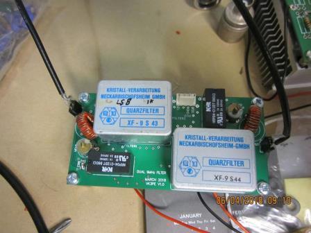
Two filters are used, as they are USB and LSB types. They are switched by the
relays on the PCB. Unused filter being grounded. The carrier oscillator then
is 9.000MHz which is crystal controlled. NOTE:
there appears to be some offset in the LSB filter as it's not offset from 9MHz
the same amount as the USB filter. This will have to be taken care of by shifting
the 9.00MHz carrier to suit. Since my VFO runs high side on all bands the
actual filter functions are reversed. ie. the LSB nominal filter becomes the
USB filter and vice versa.
Oct 2018: I am now possibly contemplating using a home made 9MHz filter. I bought a bunch of 9.00MHz crystals from eBay and then characterized them using an N2PK VNA to sort them into matched set of 8. Then use DISHAL.EXE to design a COHN filter. I swept the filter and it looks very good, 3dB BW right on 2.4KHz. But it's a big area of a PCB.
Plots and pictures soon.
March 2019:- Also, plans are afoot to use a better crystal filter than the ones shown above. This new PCB will use the Funkamateur 10.7MHz 8-pole filter, in conjuction with AS169-73 solid state switching devices.
I already have the new PCB and will show it here soon.
NEW Jan 2019:-
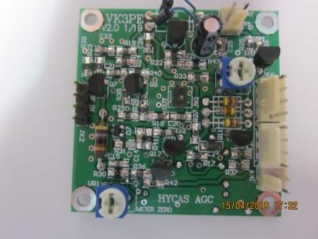
The IF section (top half of above PCB) is very similar to that published for the "HYCAS IF strip" (HYbrid CAScode general purpose AGC IF Amp) by W7ZOI, as noted above. Suggested reading is http://www.w7zoi.net/hycas-pcb.html The HYCAS AGC Sch is entirely different though. The link has schematics. The EI9GQ IF is an unbalanced output, whereas the HYCAS is balanced. It would be easy enough to connect the output in a balanced fashion to feed a HYCAS AGC if required. To that end, I have also made a HYCAS AGC board which includes an S'Meter driver. I ordered some of these as PCB's from China in Jan 2019 as you can see below. I intend to build it, along with using my IF board, but loaded to be virtually the same as the HYCAS IF section, just to compare. The beauty of the modular PCB's is that one can change sections. Coupled with the new AGC board it will represent a near copy of the HYCAS IF system. The AGC PCB is 50x50mm. The companion IF board (not shown) is also 50x50mm.
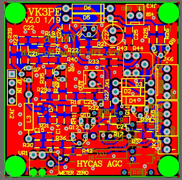
VK3PE's 'HYCAS AGC version'. Input on left side. S'meter circuitry is on rear, except for the S'meter "ZERO" trim pot.
NOTE (Jan 2019):- Readers who would like to build the complete original HYCAS IF/AGC strip, should note a single PCB is now available from Mike Hadley, G4JXX, as shown in SPRAT magazine, Winter 2018/19 edition, #177. It doesn't appear to include the S'meter circuitry though. It's not an smd PCB, all through hole parts used.
COMBINING SECTIONS ?
Once individual sections were built and tested, the idea of combing some of them into a larger (100x100mm) panel to simplify wiring seemed like a good idea.
I decided to make two larger PCB's 100x100mm each for the Tx and Rx parts of
the project to combine some of the smaller boards.. Plus the mother board for
the band pass filters (BPF) 100mm square is the 'sweet spot' for having boards
made in China.
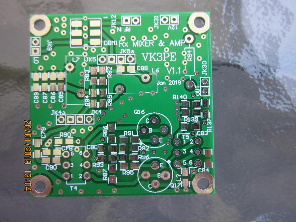
Rx "Quad" PCB. This pcb contains the IF amplifier (top left), AGC
stage, Product detector and Audio power amplifier. The audio board can use either the TDA2003 or LA4425 chip (as fitted) which requires less parts, hence the blank locations
 <<PCB is actually square.
My complete IF/AGC/Product-Detector/AF amp on 100x100mm PCB. This board, when preceded by a BPF (Band Pass Filter), the Receive Mixer and post-mixer buffer amplifier board and crystal filter, forms a complete receiver. (assuming the VFO & BFO signals are present of course)
Sch and BOM of the PCB above. NEW Dec 2020 (zip file)
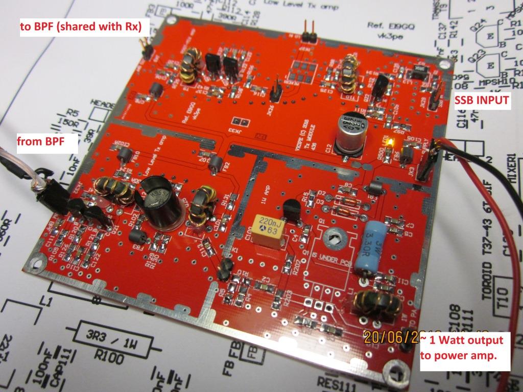
Tx "Quad" PCB: Following the idea of having several proven sections on one larger PCB, is my Transmit board, again on a 100x100mm board.
This PCB (below) contains the Transmit
Mixer, (actual mixer device not fitted in the photo) post-Mixer amplifier, 200mW driver and 1 Watt driver. The picture shows
the completed PCB apart from fitting of the smd Mixer component. (top middle
pads) The 200mW and 1W driver stages (bottom half of PCB) have been tested and
work nicely. For this build I used a 2N4427 device in the 200mW stage rather
than the 2N5109 of the PCB built previously. Results are very similar.
Of course there is more to the transceiver than
just the two PCB's mentioned above. There is also the band pass filter board
(one per band) which is shared between the Rx and Tx stages. In addition there
is the Tx balanced modulator and the crystal filters which are also shared. Plus some other PCB's, not shown here. These are covered above.
Sch and BOM of the PCB above NEW Dec 2020
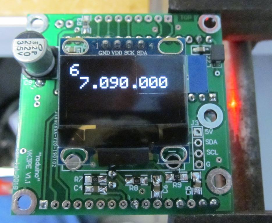
All this assumes that a suitable VFO and BFO signal are available. I use a variation of the RADUINO board, see below.
"Raduino" VFO see this page please for details.
This is the VFO I will be using, at least initially, in the project. It is based on an Arduino sketch by VK3HN. The PCB itself is my own design although it is compatible with the "RADUINO" board used in the uBITX. Fitted on the rear is an Arduino NANO board plus my own version Si5351 board which has buffer devices fitted also.
The board is 50x50mm in size and the display used is a serial (I2C) OLED type of 0.96". Other displays using this protocol could also be used with appropriate Sketch changes. (NOT available from me.)
More to come...............
HOME
Page created on 12th May 2018 by
VK3PE (see QRZ.COM)
Last updated on
December 24, 2020
Disclaimer:
I have no connection commercially nor any other arrangements with the EI9GQ Book, RSGB or ™ holders mentioned above.
The material is presented here for experienced builders and buyers of the book, to get some additional 'ideas'. No other information is available apart from that presented and it is on an as-is basis. No warranty of any kind is expressed or implied.
Other than schematics provided where I have made significant changes to the originals, readers should buy the book for detailed Schematics of all chapters..
At times I may have some spare PCB's available, subject to above.
 What started this build, some SSB crystal filters available on eBay.
  This is a partial picture of the front cover. The book was printed in 2014 &
2015. ISBN: 9781 9101 9301 3 (I have no
personal or commercial connection to the book or author, except for its purchase.) The book
is not very expensive and a great read, even if just for some ideas. I imagine
it's available via the RSGB or in some countries, from technical book sellers.
This is a partial picture of the front cover. The book was printed in 2014 &
2015. ISBN: 9781 9101 9301 3 (I have no
personal or commercial connection to the book or author, except for its purchase.) The book
is not very expensive and a great read, even if just for some ideas. I imagine
it's available via the RSGB or in some countries, from technical book sellers.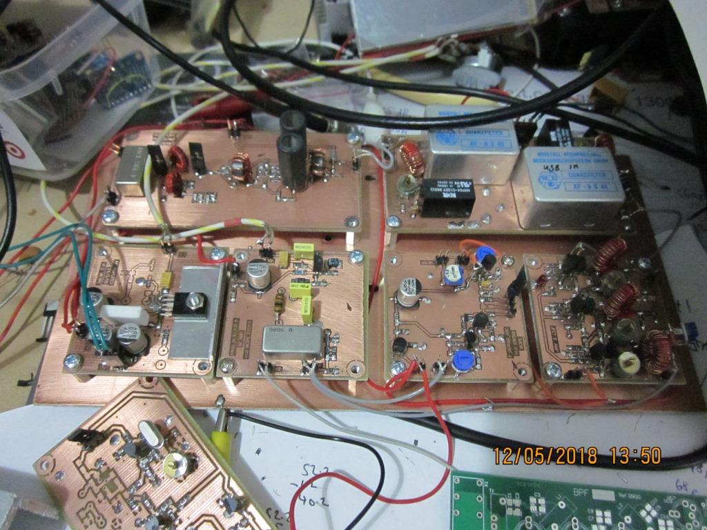 To the left, are the receiver sections. The VFO and display is not shown. Top
left is Rx mixer and post-mixer amp, then crystal filters, bottom right is the
IF board and AGC boards, then the demodulator and audio. (Clockwise from top
left) Bottom (angled) is the 9MHz crystal oscillator board.
To the left, are the receiver sections. The VFO and display is not shown. Top
left is Rx mixer and post-mixer amp, then crystal filters, bottom right is the
IF board and AGC boards, then the demodulator and audio. (Clockwise from top
left) Bottom (angled) is the 9MHz crystal oscillator board.