
Suggested Combo PICaSTAR PCB build method.
Wondering where to start?
A reminder though.......
this information is NOT intended to replace the 'official manual' which is the articles and set-up information published in Radcom originally by Peter, G3XJP, and now found only on the Yahoo 'picaproject' group.
Last updated on Jan 30th, 2014:- [loading of the MAX232 should be done, before fitting the ADSP-2181 or the LED may not flash]
CAUTION, FOR Combo "P1 & P2 or P2a" version builders, some of these notes may not apply.
Sept 2, 2011, added link to Beeper assembly in the text,
(Nov 15, 2010: changed the DSP test to incorporate the official manual procedure and corrected star directory screen shot)
( Jan 17th, 2011, , March 25th 2010, new integration section )
** Presented in good faith but content subject to errors and ommisions. **
This is a fairly complex project and one where it's easy to lose faith in your abilities and give up before completion. Especially if you have not tackled anything like this before. eg surface mount parts fitting.
This is a 'homebrew' project and is NOT a "kit".
There is no step by step component placement document.
There is no parts kit available.
YOU have to source all parts yourself and follow the schematics for assembly.
YOU must read and use the "Manual" by G3XJP, to commission your new radio.
Below, is VK3PE's guide for assembling the Combo PCB's in blocks. It is not the only way.
There is NO detailed fault finding procedure here. If things don't go to the plan below, you need to debug it.
If you are already experienced though in PICaSTAR builds, then no need to read further. < Back>
Here is my own method of attack:- ( I suggest you read all of this before soldering anything though) It is NOT a complete guide to building. It assumes you have read Peter's information and basically have some understanding of what you are doing.
These pages assume you have all of the parts to hand. This obviously may not be the case, so feel free to load parts as you get them but as you will see below, my preference is not to load any IC's until the various voltage regulators have been fitted and checked.
I like to build and test as I go. I also prefer to fit smaller parts first along with the associated regulators. Then the PCB can be powered up and the various voltages verified. Also, various blocks can be assembled and tested, one at a time.
When directed to apply power, best to use a power supply of fairly low current rating (eg 1amp or so) and with a current meter capable of reading in milli-Amps.. A current limited supply may help but is no guarantee of avoiding problems. NOTE, reversal of power supply will most likely destroy your good work. If in ANY doubt of your attention span, place a series 1A diode in the positive lead AT THE PCB END. ie solder the cathode (bar) to the +ve point on the PCB, and a red wire to the anode which connects to your power supply.
As you build, it's a great idea to check for shorts between pins using the beeper which was designed to avoid damage to the IC's as it has a very low voltage output. The PCB for that is on the panel and well worth building as the 1st SMD pcb and a great tool to have.
To speed up the loading of the PCB, I have the component overlay (pdf) by values, (Hi-resolution) up on my PC and zoom in on an area being loaded. That way you can quickly see the values to be loaded.
If your PC is not handy to the workbench, open the file above then zoom in on the area you are loading. (About 1000% is good) then print using "Current View" to print out that section only.
I find it best to load all of the 100nF caps, then the 10K resistors as are they are in the majority. You do need to be organised though with all of the components on the (clean) workbench.
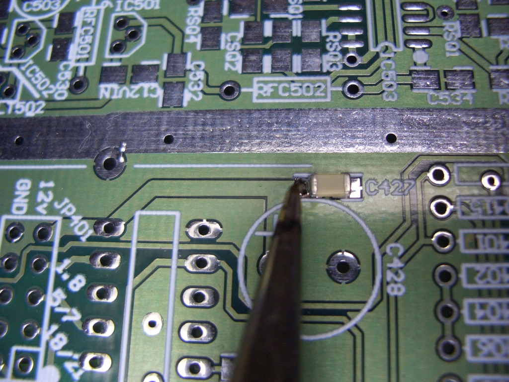
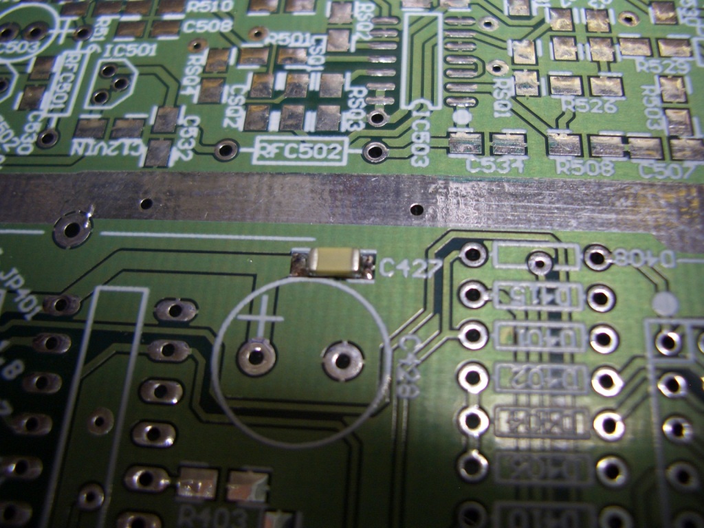
When soldering SMD parts, only a little solder is required. Resist the temptation to put lots of solder on each part. Just a small fillet of solder is plenty.
To solder SMD caps and res., lightly tin one pad only. Hold the part with tweezers in place and wipe the soldering iron across the end just tinned, at right angles to the end, with the iron in touch with the part and solder. It should reflow the joint. Don't keep the iron there for longer than required to reflow. Then, hold the end of the solder across the other end of the part and wipe the iron across the end and the solder at the same time. When the solder melts, remove the solder so that not too much solder makes the joint. A small fillet is all that's needed.
It's hard to put into words, pictures below may help:- 1206 part is shown. 0805 is 'easier' and is preffered for VK3PE's PCB's.
< click for larger size >
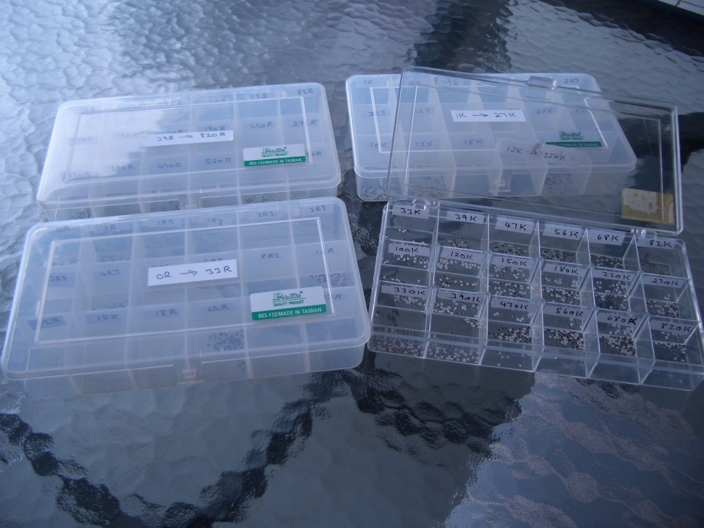
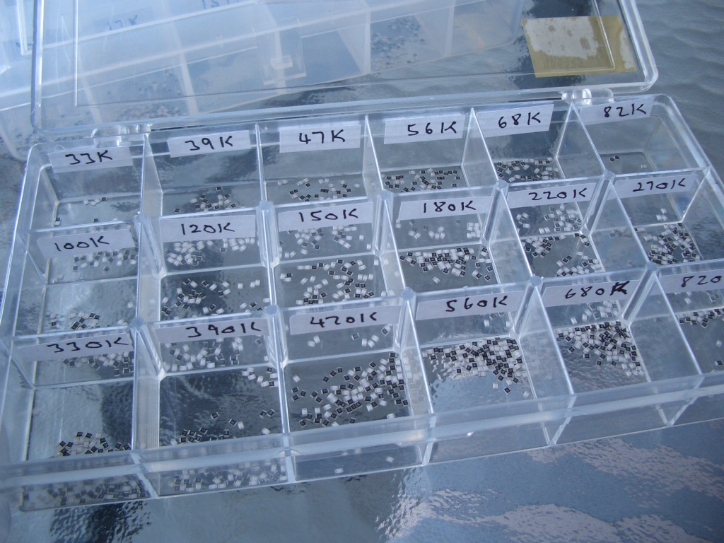
I keep my resistors in some cheap plastic containers. Four of them hold most values and sitting on the workbench, it's easy to get the values you need, using your tweezers. These are all 0805 parts from 'Sureelectronics' on eBay. Sticky lables identify each part. NB. The Sure kits miss some common values of resistors. Their kits also may not provide sufficient QTY of each value for Star building. eg 10k
Audio Amplifier
One of the easiest sections to build and test is the Audio Amp. IC902. Assemble all of the parts of the AF amp, shown on sheet number 6. (the sheet numbers are in the title block of the Combo BB schematics). It is best to trim back the Amp's pins about 1-2mm before soldering the device on. Solder the tab also to ground. Plug in stereo speakers to Jack 1. Then, power up the PCB by connecting a 12-13v DC power supply to the "switched DC" area tabs. No need to fit the tabs, just solder a temporary wire (+ve) to that area and the Gnd (-ve) to a convenient ground point nearby (say, in the BPF area.) At power up a slight click may be heard in the speakers and the current drawn should be about 16-20mA (after an initial surge when charging up the caps.) Place a finger on each input and a 'buzz' should be heard in the speaker. Current will rise also. OK, that section is working !! Feels good. Make a cup of tea/coffee and reflect on your good progress with your XYL.
RS232 area
Next step is to fit the MAX232 device and parts. IC21. You should also fit the rear toggle switch and DB9 connector. Power up again (10v) and check the voltages on pins 2 and 6 of IC21 with reference to ground. They should read about -9 and +9v. Don't be fussed if it's a bit higher or lower.
ADSP-2181 area
Now, wet your feet on a larger SMD IC, the ADSP-2181. This has fairly wide spaced leads and with care is easy to solder. BUT, solder in only the SMD and through parts around that area, including the regulators. Refer to sheets 3&.4. You can also fit the parts on sheet 4 except the CODEC. (Leave out C95 and C96 though as they will make fitting the CODEC difficult later) Now, to test all is well (NO ADSP2181 or CODEC fitted! ) Adjust your power supply to about 10V and connect it to the anode end of diode D34B (marked "10v") Gnd lead as before. Turn on the power supply and CHECK all of the voltages are correct. NOTE, there are two regulators on the PCB for the 3v3 supply to the CODEC Fit one only ! The LM317, if fitted, also has some parts under the PCB.
Now, you fit the ADSP-2181. If this frightens you....... find an old PC card you have been hoarding away and see if there are some similar IC's on it........ Try soldering the pins and removing the excess solder again with Solder Wick, for practice. Place the Solder Wick over the end of the IC pin and PCB pad area. If you put the wick up higher, the pressure of the iron may bend delicate leads. Any bridging up the side of the IC will flow into the wick also, with practice. Once you are happy or confidence boosted, you can now solder on the ADSP chip.
Lightly tin one corner pad on the PCB only. Now place the ADSP into position making sure that pin 1 alignment is correct. i.e. it's the right way around. Make sure all pins line up. Best to do this by looking directly over the top of the part, holding it down with one hand, with a small screwdriver end, or your tweezers. Then with the other hand, re-flow the joint while maintaining the downward pressure. Then, solder the opposite corner but ONLY if its still aligned. Check again, then you can solder all of the pins. I like to use thin (0.355mm) for this. Remember, you only need a small amount of solder. The iron is best held at the end of the pin, with contact also to the PCB pad. Dab the solder to the iron and it should flow onto the pin and pad of the PCB. Do this fairly quickly, to avoid PCB damage. Go round all the pins. Don't panic if you bridge solder to the next pin, keep going. Then, using the solder wick, clean up any excess solder. Since you practised on the old PC board, this should be easy ! Use the beeper to check for shorts between pins. Then fit remaining parts.
You need a 27C512 (or a 27C256 will work) programmed with GMON.HEX from Peters Yahoo "picaproject" pages, for IC126, mounted in a socket, preferably. Now, you can apply the 10V power to the section as before, to D34b. The current will be in the order of 120mA and you should be greeted with a flashing DSP LED !! (if not, is the LED inserted correctly, ?) More progress....... Maybe another cup of tea/coffee. {For more details, Refer to Peter's document "STAR_06.pdf". See the section titled "hardware test"}
About now, you may be wondering just what the flashing LED means ? The EPROM, loaded with "GMON" contains a bootloader. This is simply a program that "starts" the DSP process. All it does is to ready the DSP chip for communication with the outside world, via the serial port and when it has done this, flashes the LED, signifying that it is ready to load the DSP code.
CODEC
The CODEC, IC26 can now be fitted. For the optically challenged like me, invest in a head band magnifier or bench light/magnifier for this work. In fact I use one all the time. Fitting is the same method as the DSP, but you need to be much more careful this time as the part is tiny. Take your time getting it aligned and tacked each corner. Check and double check ! Then, solder all the pins and don't worry about bridging again, as you can simply remove the excess with solder wick. (You did practice this ?) Do not press the iron too hard onto the solder wick and the pins or the pins may be bent. They are quite fragile. Your Solder Wick should be of good quality and fresh. Some cheap solder wick has little inbuilt flux and is hard to use. Older wick dries out. Beep out all the pins when done to check for shorts. You must do this !
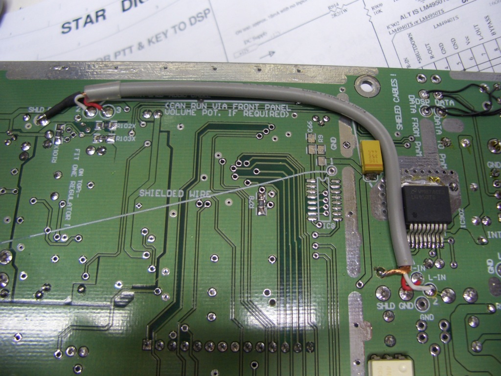
Make up a cable using twin core shielded audio cable to run from points 2 & 3 under the DSP section, to the AF amp section. If you have heat shrink tubing, fit it over the shield wires for a neater appearance also. Route it between the parts shown and it will stay in place. In the picture below, I scraped the PCB to solder the braid in a slightly different place, at the Amp end. You can do this or use the nominated GND point though. Don't overheat this type of cable when soldering or you run the risk of the braid shorting through to the inner wires.
Timer
Next, install all of the Timer parts, except the IC's again. Connect 12V to the DC Power tab area again and check that the timer's 5v regulator is working. If OK, install the ULN2803 and a socket for the PIC, then the actual PIC16F627 (programmed with "STVOX04.HEX" from Peter's G3XJP's Yahoo Picaproject pages, OR, if you will be using Ian's Peak SWR meter, use Ian's special Timer code). Re-connect 12V:- the 10V and 12v Rx LED's should light. The 12v Tx should NOT be lit. If it is, there is a fault in the timer area or the PIC is not programmed. Note that the timer's 10V supply will be powering up the DSP area also and the DSP LED should be flashing.
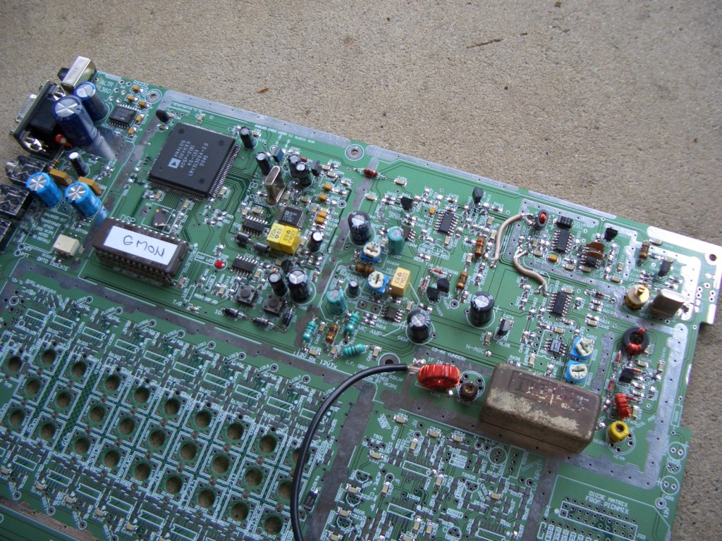
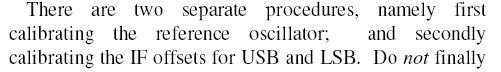
Your board should now look something like this picture:- < click to enlarge >
Now is the real exciting time....... Getting the DSP working !
IMPORTANT:- Testing of the DSP section
You MUST now refer to the set-up information contained in the picaproject Yahoo group. You need to download the test programs there and also have a copy of QBASIC™ compiler. This can be obtained as freeware and runs under DOS™.
May 8th 2016 QBasic LINK no longer works so removed: Goto picaproject Yahoo Groups, files area, should be in the DOS Boot Disk ZIP file now
. QBASIC Using QBASIC, You need to do the following:-
Run QBASIC.exe and open the "xx.bas" files as directed. Press F5 to run the program. Follow the on-screen prompts.
The next section assumes you have the DSP code and parameters on your hard drive (From Peter's {G3XJP} Yahoo group files and loaded onto your PC per his instructions)
 These
files should be in the C:\Star2b directory. Plus
QBASIC.
These
files should be in the C:\Star2b directory. Plus
QBASIC.
(QBASIC is aso available on the picastar-users group.) If you change the directory name from Star2b, then you wll need to edit the "xjp.ini" file with Notepad, to reflect the change. Names should be 8 or less characters.
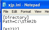 xjp.ini file
Connect a cable from the PC serial port (COM1) to the DB9 on the Combo pcb. You should have speakers plugged in also. (Above left picture)
Place the switch at the rear to left position. (Closest to DB9 Conn.) Refer to my schematics and also Peter, G3XJP's, "RS232_mod.pdf" file (in the picaproject group) in order to understand what hapens to the RS232 signals to and fro from the xjp Loader (XJPld2g9.bas) program if that is used for the intial setup. There is also another loader that may be used. Alessandro, IK6FWJ, has a loader which is also availale in the Picaproject group files area. This is MS Windows based. "Loader StarII.exe" Vers. 5.4 should be placed in the irectory above also.
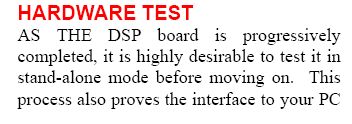
* Run XJPld2g9.bas using QBASIC Refer to Peter's document "STAR_06.pdf" for details. See the section titled "hardware test". Below is a snippet of the document to guide you to the correct section.
There is some basic fault finding information there also if things don't go to plan. Carefully check your connections, power supply voltages, track continuity etc also.
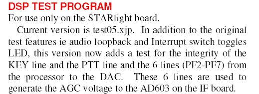
You should also check the AGC operation (option 5 in the program). Refer to "CH2_Rev 5.pdf" DSP TEST PROGRAM paragraph. Below is the 1st paragraph only.
 "STARlight
board" is PICASTAR DSP.
"STARlight
board" is PICASTAR DSP.
The other test (AD603 IF GAIN calibration) should be left until the receiver is completed. See section after BPF.
Once all is well above, you could also try loading the DSP code, to hear the Morse "Hi" showing that the DSP code has loaded. Normally, the DSP code is loaded using QBASIC in a similar fashion to that detailed above. The procedure is detailed in the "CH2_Rev5.pdf" document. If successful, you will be greeted with a Morse "Hi".
{ ensure that C658, Cx58a, Rx58a and RFC607 are fitted, if you don't hear the "HI". They are shown in the IF Schematic } >>> added 5th Feb 2014
There is also another way to test the DSP code loading, if you install Ian, G3VPX's, Hobcat (Google G3VPX) software on your PC. "HOBCAT" is primarily for the Trxavr PCB but also has the facility to download the DSP code using the serial port. Some may find this less hassle due to PC problems with the long DSP load sequence. NOTE, this method does NOT do loopback or the AGC test of the DSP/CODEC detailed above, so if you have a problem loading or find AGC is not working, you MUST go back and do the hardware tests shown above. To install Ian, G3VPX's "Hobcat" program, See this link for HOBCAT
Install and run Hobcat and use "Setup" menu to select the Star Folder you made on the PC. Then select the Parameter file, User2b2.xjp. Power up Combo again and LED should be flashing. In Hobcat, select the menu item Tools/DSP direct loader(comport) Click on "proceed". You should see a counter running in Hobcat AND the DSP LED should stop flashing and be mostly on but perhaps a little less bright. If so, the code is loading ! When the count finishes at 19900 you should be greeted by "Hi" in CW and the LED will go out < Ref Part 6 of Peter's document >..........Congratulations. YOU have loaded all of the above parts, AND loaded the DSP code ! Well done. Celebration time, have another cup of tea/coffee or maybe something stronger this time, YOU are making excellent progress.
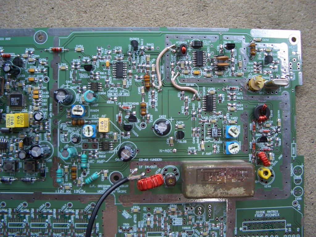
IF Amplifier
Load the IF section, again checking voltage regulators before fitting any IC's. I am stressing the importance of load, check, load parts. It will pay dividends if you have any faults. Then, check the DC voltage at the output of the TL072's, it should be close to 5v. Similar for the AD603. When the IF section is fully loaded and you re-load the DSP code as before, the background noise level should rise, indicating the IF is 'functioning'. (set the trim pots in a similar position to that shown in the picture to the left, below) Obviously this is not a full test of the IF section nor are the Pot's in their final position. That will come later when you have the receiver running and do the Calibrate routine (CAL_IF) according to Peter's instructions. < Parts 8 & 9 > I used a signal generator and fed it into the IF input and peaked the 2 trimmers. (These are best adjusted for best matching, least ripple) Sensitivity was about -130dBm.
Butler oscillator and amplifier section
Load the Butler oscillator and amplifier section. Power it up, check voltages are OK on regulators and adjust the Butler to suit the crystal you have. All of this is detailed in Peter's documents, < Ref Peter's Part 14 > however, it refers to the old version of DDS IC so you need to also refer to the later AD9951 document for winding the transformer in the DDS area.. The DDS carrier section can be loaded also but again, do not load the actual DDS chip (AD9951) until you have checked the 3 voltage regulators.
The toroid fitted in the DDS filter section here is temporary. On the version with "Bob's Mods" fitted, the values in the DDS filter are different to what is shown here. The 2N3866 is also replaced with an MMIC device for more consistent output level.
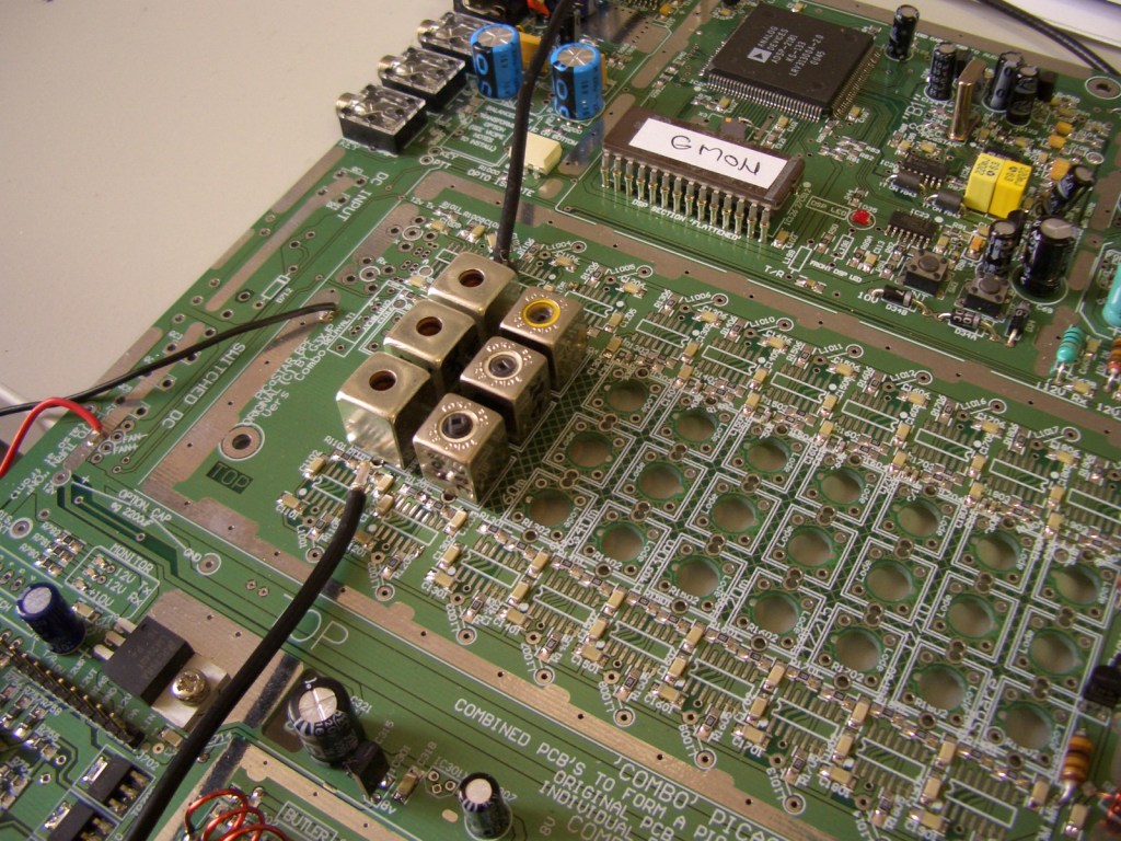
Magic Roundabout (Rx & Tx mixer)
Load the Magic Roundabout, again checking voltage regulators before fitting any IC's. < Ref Peter's Part 16 & 17 for general information > There is also an alternate regulator here using the LM317 so fit one only. The four J310's are best matched before fitting. This is only practicable if you have a reasonable number of the devices to sort through. Join the gate to the source and connect them to the negative of a 12v supply. Fit a mA meter in the drain to power supply positive. Note the current. Typically it will be between 20 to about 35mA. Check a number of devices and select 4 with close currents. If you only have 4 parts, them use them as is. I did this on this PCB build. These devices run quite warm to the touch. This is normal. < I later found some T092 flag heatsinks at a Hamfest (March 14th) and fitted them. >
On powering up again, check all the voltage dividers (using 2k2, 2k2) for half the supply voltages. This is a rough check that nothing is amiss. Use Peter's information for setting the 500K trim pot later, when the DDS signal is available.
You can also fit the co-ax cables under the PCB at this stage. Use the highest quality co-ax you can here, for best shielding. The mini Teflon type co-ax is the preferred type if you can get it, as it has good shielding properties. Sometimes you can buy a few meters of this, on eBay.
 NOTE:
the DDS filter section has not yet been loaded so the cable from the DDS Amplifier,
bypasses the amp and runs directly to the MR local Oscillator input. The black
co-ax is a temporary receive input signal for testing. (ie bypasses the BPF
which is not yet fitted)
NOTE:
the DDS filter section has not yet been loaded so the cable from the DDS Amplifier,
bypasses the amp and runs directly to the MR local Oscillator input. The black
co-ax is a temporary receive input signal for testing. (ie bypasses the BPF
which is not yet fitted)
At this stage, you could divert to building the Trxavrb PCB and use it to control the Combo PCB, in the above build state. It will allow you to control the DDS and actually get the receiver to "work".

8th March, 2010: At this point, I connected a spare Picnmix to control the DDS and loaded the DSP code using Hobcat again. Lo and behold, the receiver operates. I have sensitivity of better than -135dBm. (this will reduce when the BPF is fitted, due to additional losses)
Diode Matrix
Load the Diode Matrix. The 2nd ULN2803 and "Band" LED's are optional, but recommended, as they give a quick feel for the state of the controller and add some "bling". Note, the WB LED is fitted the opposite way round to the other LED's!
The Band Pass Filter
The Band Pass Filter section can be loaded now if you wish. The Picastar will function as a basic receiver without it, and it avoids winding all those coils until later! < Ref Peter's Part 18 & 19 > You need to use the Official Modification List on Peter's Picaproject re filter values. These are reflected though on my documents (BOM and Schematics) for Combo PICaSTAR.
BPF Coil winding: Lodestone information (Excel spreadsheet), Toko information. (See links within) What I like to do (after having wound several sets of these already) is to wind one band set at a time. Then adjust them to the nominated inductance using an AADE inductance meter. (a kit is available for this very handy meter) Mark the side of them with the band, 'active' pins and put them aside.
Start to load the BPF area. Again, load the 100nF caps and 10k Res first then the other parts. Do not load the FST parts or the coils yet! Don't forget to load the parts underneath also. Tuning parts are 0603 types.
Make sure you load the right parts ! It is VERY easy to mix things (parts) up here. Load ONE band at a time, before moving to the next band. If you mix the parts, even one, it will be very hard to find later as the band will not tune and you will be faced with removing all of the parts and replacing them.
You can then power up and check that the 5v regulator is working. Fit the FST parts and finally, the coils. Make sure you fit them correctly, with the winding in the right orientation. When fitting the coils, I like to fit one band at a time and check the band tuning, using an N2PK VNA. You may not have this facility of course. This means that you must have the controller running, to select the bands. I also only lightly tack solder each coil into place in case it needs to be removed again. (In case you wound it incorrectly or mixed up the coils .....hence my note re marking them !)
Eventually, you will have all the bands fitted and working. If you don't have a VNA or can't find a friend with a VNA to help, then it is more difficult. I do suggest having the AADE meter though and pre-tuning the coils. Most bands will then need little or no tuning.
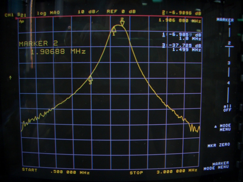
Here is the 80M band swept on the VNA with the Toko coils set to correct inductance on the AADE meter.
You can see it is fairly close initially, but I think the tolerance of the 1nF caps used may have a big effect on the result. I checked some of the 1nF caps. in my parts bin. (They are most likely not NPO types) and found they ranged from 910 to 933pF. This probably accounts for my filter being on the high frequency side. Some 0805 parts checked were very close to 1nF (1000pF).
Here is the filter after tuning on the VNA. Not too bad. You can also possibly tune the filters by peaking all on a signal in the middle of the band, then look for a signal each end of the band and tune one outer coil, then the other. Refer to Peter's manual though for information on tuning. There are other ways also, eg a signal generator can be substituted for the on air signal of course.
Just as a matter of interest, my 160M coils were wound using Lodestone formers and pre-set to the required inductance. Sweeping the filter resulted in a near perfect band pass with no adjustments required. Click picture below for more detail.
The 160 & 80M bands have been installed in this description. As you can see above, there are no FST parts in place yet. I swept the filters by connecting directly to each filter. As per previous sections in this description, I like to install and test. So, carrying on, the 80 and 20M bands were wound, measured and swept. I found that these bands needed a little tweaking, maybe +/- half a turn on each coil. Then, the FST parts were fitted. (I don't plan to install any more bands at the moment.)
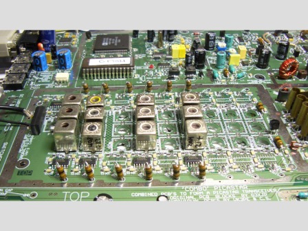 A co-ax cable was then fitted underneath to join
the output of the BPF with the input of the MR. A temporary co-ax was also fitted
to the Rx input area. (Visible in above picture) There is provision for an SMA
type socket here but I generally just solder a cable on. Keep the inner section
short. You can run the cable on the top or bottom. Bottom is better if your
LPF board is located underneath. Same goes for the Tx cable. { In my build,
Combo PCB is located under the chassis on 10mm high spacers. That space is also
used for the bottom shielding. But there is also room to run co-ax cables under
plus the DSP serial cable < use twin shielded > You can use longer spacers
if you have the room.}
A co-ax cable was then fitted underneath to join
the output of the BPF with the input of the MR. A temporary co-ax was also fitted
to the Rx input area. (Visible in above picture) There is provision for an SMA
type socket here but I generally just solder a cable on. Keep the inner section
short. You can run the cable on the top or bottom. Bottom is better if your
LPF board is located underneath. Same goes for the Tx cable. { In my build,
Combo PCB is located under the chassis on 10mm high spacers. That space is also
used for the bottom shielding. But there is also room to run co-ax cables under
plus the DSP serial cable < use twin shielded > You can use longer spacers
if you have the room.}
That's about it for the Combo PCB build. To use the Combo PICaSTAR though, requires a 'controller'. In this case, the Combo panel is supplied with a Trxavrb PCB so that would be the suggested next assembly. Some of you may have a PICnMIX, either home made PCB's or from one of the previous "panels". You can certainly use PnM if that is what you prefer. You will need to make some cables of course, starting at the Combo PCB with IDC cables and terminated individually to suit PnM.
Once you have built the Trxavrb, you can connect it up and have a listen on the bands ! But, you will need to set up the Butler Oscillator frequency and IF offsets. You MUST use Peter's manual for this. "Ch2_Rev5.pdf" Partial view below
Finally, go back to "CH2_Rev 5.pdf" and do the AD603 GAIN CALIBRATION. Also, see the section "RECEIVER HARDWARE GAIN" to adjust the post between C62 and C18 on the IF section. "RV604" on the Combo PCB.
NOTE: If you plan to fit a TFT display (colour) then the Encoders 8 section is also available on the new TFT PCB. This means you don't need to load the 2nd Atmega device on the Trxavrb PCB.
Being impatient, I set-up my spare PICnMIX and tuning Encoder from Star #1 and adjusted the Butler Oscillator values in PICnMIX (See Peter's notes re DDS command "933" ) This tells PICNMIX (or Trxavrb) the exact Butler frequency so your frequency display will be correct.
Briefly, what I did (and explained in RTFM) was key in "83" for Sig Gen. mode, then "88" for keyboard frequency entry. I selected 25MHz. and then monitored the output of the DDS amplifier with a Frequency Counter. Peter's command "33" is then keyed in and the display will be 'locked' at 25.0000MHz. (a higher frequency would be even better) The tuning encoder is then adjusted until the exact frequency (25.0000) is displayed on the counter. [ Lacking a counter, use your general coverage receiver, calibrated of course ] Then key in "933" and it is written to memory (EEPROM). These are DDS commands and the 1st key must be a 'long' press. RTFM ! { This method assumes you are reasonably close to the frequency already. You should initially use Peter's set-up program in Qbasic to key in the nominal Butler frequency}
Then, I could tune around for signals. I set it up on 80M and plenty of signals about. You can see my "breadboard" style setup below in receive mode. Although the 2 band pass filters are fitted, they have not yet been connected so all receiving is with no BPF in place at the moment.
Click on the picture below to hear a QSO on 80M ! < 17th March, 2010 >
 Click for QSO !
Once you have the Trxavrb built, you can finish off the main board. Fit the DC tabs for connection to the board and the reverse polarity relay. The on/off switch can be connected to two places on the board.
1) at the rear, adjacent to the relay. 2) at the front left corner. Of course, if you don't want to use a switch, just link across with a short wire.
There is an integration drawing on the ComboBB page. For "P1 & P2" Versions, see here.
Shielding:
There is provision for extensive shielding on Combo board. I suggest you resist the temptation not to fit them all ! It is a little tedious to make up the shielding walls and covers but it will pay dividends in the final radio. There is some information here on a suggested way to make the shields .
However, I suggest you have the whole transceiver operating before you fit all shields or at least don't solder on the covers.
PA boards and Low Pass Filter
Leave the PA boards and Low Pass Filter to the very last. They can't be used anyway until the Trxavrb PCB is assembled. Details however, for assembly, are on Steve, G6ALU's web pages. You can also refer to my previous build pages for LPF, the 20W PA and 140W PA's.
Integration
There is an integration drawing on the ComboBB page. For "P1 & P2" Versions, see here.
Internal speakers. There is provision, under the PCB at the rear, to connect internal speakers if you wish. These will be switched off if the rear 3.5mm jack is used. ie. External speakers are plugged in.
Microphone and PTT. There are points under the PCB (marked in text) for these connections. Run a shielded cable for the Microphone to your chosen Mic. Connector. It might be advisable to fit a ferrite bead and small value Cap. at each end.
Power amplifiers, Bias.
Power amplifiers, DC supply.
Low Pass Filter.
DC supply.
Trxavrb. It is advisable to keep the control IDC cable under about 150mm in length. Some have reported intermittent DDS operation with long cables. Poor grounding between the assemblies can also be a factor.
NOTE: If you plan to fit a TFT display (colour) then the Encoders 8 section is also available on the new TFT PCB. This means you don't need to load the 2nd Atmega device on the Trxavrb PCB. The Tft PCB is available from Gerard, VK3CG for about AUS$5 plus postage. Gerard may also have soem of the IC's that are used on the Tft board.
This section not completed.
Happy Building !
VK3PE
Trxavrb
To make the board function though as a receiver, you do need to also build the Trxavrb control PCB. It is the densest board and the assembly above should have given you confidence to tackle it. Again, it's load, test, load. In this case though, only load the 5volt regulator parts and check the supplies first.
NOTE: If you plan to fit a TFT display (colour) then the Encoders 8 section is also available on the new (to be announced) TFT PCB. This means you don't need to load the 2nd Atmega device on the Trxavrb PCB.
I suggest you follow Ian's information on his web pages very closely, especially the programming sections, in order to get this PCB running without any trouble. You will need the included PONYPROG PCB to program the Atmega's on this PCB.
Ian has a procedure to load a minimum of parts for a functional test. Refer to TrxAVR PCB by Ian, G3VPX
See VK3PE pages also for further information re BOM, Schematics, overlay, etc..
This is the point where you also need to decide what display you will be using, although it's not set in stone.
You can elect to fit a cheap and simple display initially and change later to graphic or even colour as your finances or whim changes. If making, buying or adapting a case, keep in mind the final display type you may use as this will dictate the size required.
You can even make your case from PCB material, like original PICaSTAR. An example of this construction is shown here, by Charlie, VK3NX. Look out also for a suitably sized obsolete test instrument at Hamfests, Ebay etc, which might suit your STAR. This is the approach I have taken.
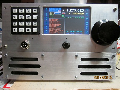
November 2010: Using a commercial case. This is usually the easiest way to overcome the housing of a new project PIC-a-STAR. There is still work involved of course. A case large enough to house Combo pcb and ancillary parts is needed.
Some pictures of a typical case............ This one is an old error tester from the phone industry. These are now obsolete and there are many makers of them. They are usually quite cheap as they have no life for their original purpose. You may even find a few parts inside that you can re-use for another project. There are other examples on the builders pages (a link is on the main Combo B web page)
Usually, a chassis can be fitted after the case is stripped of parts, to mount the Combo board. Mostly, people fit the Combo PCB under the chassis as this lends itself to easier mounting of the PA'sand LPF on top.
 This is a P1 PCB version.
To be continued ! Check again. Various sections may be added to.
Ian, G3VPX's web page
Steve, G6ALU web pages for PA's and LPF
Created by VK3PE on 27th Feb, 2010